A research group led by Professor Hiroshi Amano and Associate Professor Atsushi Tanaka (specially appointed) of the Institute of Materials and Systems for Sustainability developed a lossless short-time laser slicing technique for GaN1) substrates in cooperation with Hamamatsu Photonics K.K.
Monocrystal GaN substrates are indispensable for high-performance devices using GaN substrates. However, the high price of GaN substrates prohibits their widespread use. The achievement of this study will lead to a significant reduction in the fabrication cost of devices using GaN substrates and their increased use in society.
Part of this research was conducted under contract of R&D for the expansion of radio wave resources (JPJ000254) and strategic information and communications R&D promotion programme (JP215006003), organized by the Ministry of Internal Affairs and Communications, Japan.
[Points]
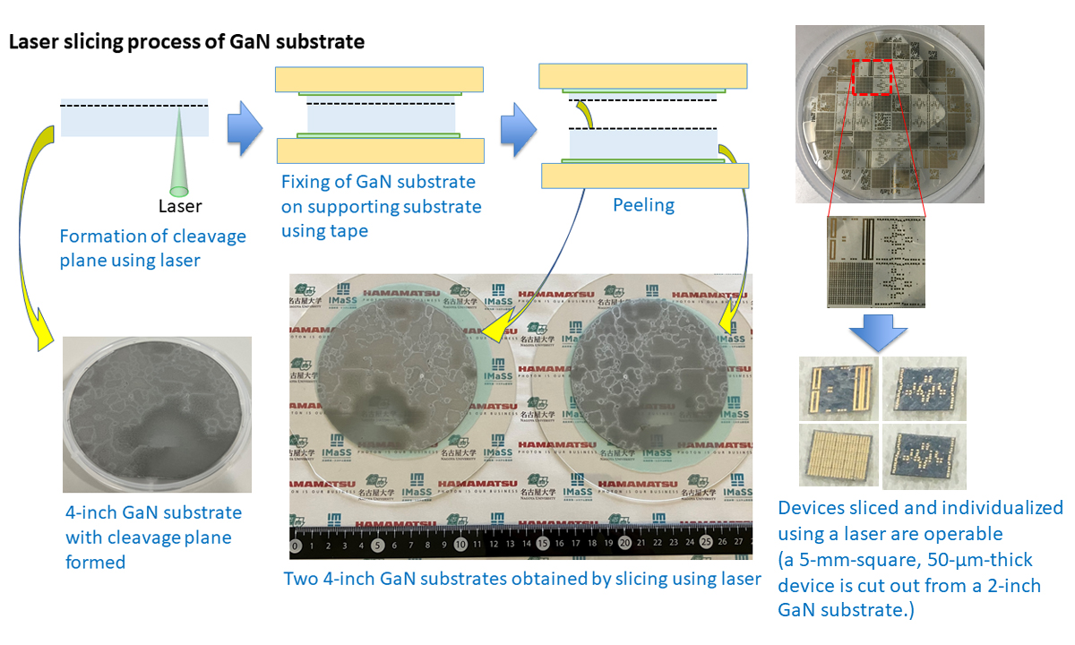
- The loss of expensive GaN crystals during slicing is suppressed because GaN substrates are sliced without the kerf loss (space for cutting) resulting from using a laser.
- Slicing without using a wire can reduce the waviness of the cut surface and produce a smooth surface, reducing the need for polishing and grinding processes after slicing.
- Extremely hard and fragile GaN substrates are cut at a high speed.
- It is possible to slice only the fabricated device layer from the back side of a GaN substrate by irradiating the GaN substrate with a laser that can pass through the substrate. The devices obtained by the slicing method can operate normally because the technique does not produce large vibration or stress.
[Glossary]
1)Gallium nitride (GaN): GaN has high-performance characteristics as a power semiconductor and is commonly used as a light emitter in LEDs and other devices.
[Reference]
Related published journal papers
"Smart-cut-like laser slicing of GaN substrate using its own nitrogen"
Atsushi Tanaka, Ryuji Sugiura, Daisuke Kawaguchi, Toshiki Yui, Yotaro Wani, Tomomi Aratani, Hirotaka Watanabe, Hadi Sena, Yoshio Honda, Yasunori Igasaki, Hiroshi Amano
Scientific Reports, May 31, 2022
DOI: 10.1038/s41598-021-97159-w
URL:https://www.nature.com/articles/s41598-021-97159-w
"Laser slice thinning of GaN-on-GaN high electron mobility transistors"
Atsushi Tanaka, Ryuji Sugiura, Daisuke Kawaguchi, Yotaro Wani, Hirotaka Watanabe, Hadi Sena, Yuto Ando, Yoshio Honda, Yasunori Igasaki, Akio Wakejima, Yuji Ando, Hiroshi Amano
Scientific Reports, May 31, 2022
DOI: 10.1038/s41598-022-10610-4
URL:https://www.nature.com/articles/s41598-022-10610-4
Principal Investigator
Designated Associate Professor Atsushi Tanaka,
Institute of Materials and Systems for Sustainability, Nagoya University
Website for Amano Laboratory
http://www.semicond.nuee.nagoya-u.ac.jp/english/index.html