CIRFE
Organization
Center for Integrated Research
of Future Electronics
Center for Integrated Research of Future Electronics
Director
AMANO, Hiroshi
The Center for Integrated Research of Future Electronics (CIRFE), established in October 2015, engages in leading-edge electronics research-including research in the untraversed area of devices with gallium nitride, carbon nano-tube, SiC and other post-silicon materials-while also cultivating top-notch human resources to lay the foundations of the future electronics industry. CIRFE is divided into six sections, each staffed with instructors who serve as leading specialists in their field, and equipped with outstanding research infrastructure. The Center’s fully integrated joint research and education system covers everything from basic scientific education on materials, measuring, devices, and applied systems through to the completion of student educational courses. Through research on energy-saving devices, an area in which very little experimentation has been carried out anywhere in the world, CIRFE strives to foster well-trained human resources who will lead the field of manufacturing in the twenty-first century.
CIRFE
![]() Movie
Movie
CIRFE Introduction video
-
Amplify the passion for the future(2min.40sec.)
-

Short version(2min.)
-

Long version(12min.40sec.)


 Section / Group
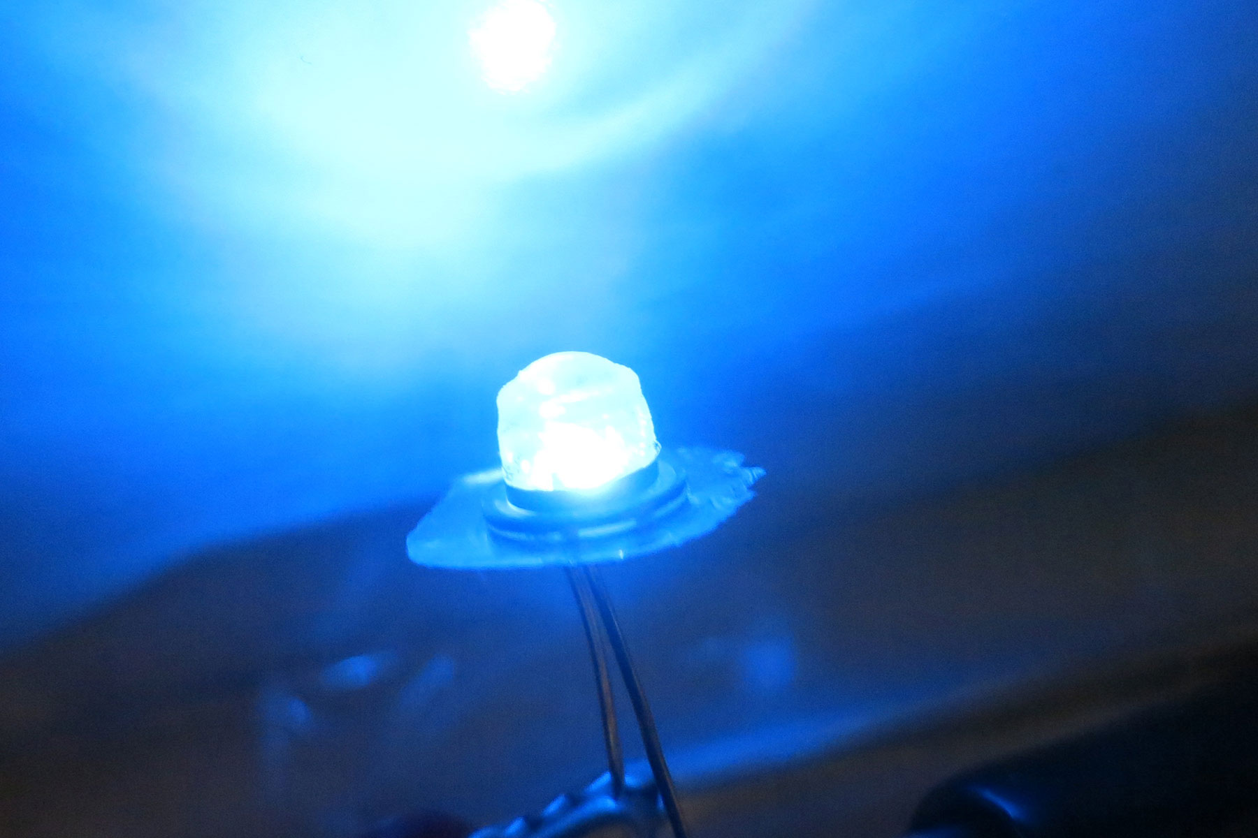
Device Innovation Section
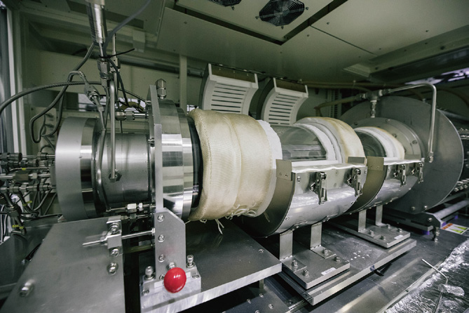
The Device Innovation Section aims to develop devices with new functions by establishing new crystal-growth methods and process development for cutting-edge electronics materials with a central focus onwide-bandgap semiconductors and ultrawide-bandgap semiconductors, such as gallium nitride, silicon cable, aluminum gallium nitride, and nanocarbon materials. A fully integrated research approach enables us to establish a unified process from crystal growth to device design, manufacturing, circuit dedign, and assessment.
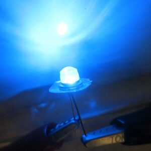
Prototype of Blue LED
-
Crystal Growth (Amano Lab.)
-
Nanomaterial devices (Ohno Lab.)
-
Energy Conversion Device (Usami Lab.)
-
Semiconductor Engineering And Integration-science (Miyazaki Lab.)
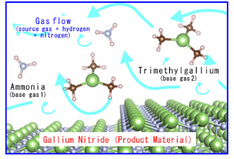
Crystal Growth
To realize gallium nitride and aluminum gallium nitride semiconductor devices that will serve as the foundation of next-generation electronics, we carry out a wide variety of research from the growth of bulk crystals for use as substrates free of killer defects to the growth and processing of next-generation quantum structures and nanostructures.
Member
-
Project
Generation of noble nitride-based devices and their contribution to the development of new infrastructure
-
Project
Creation of sophisticated devices based on Nitride semiconductor
-
Project
Study on nitride semiconductor crystal and devices
-
Project
Creation of Next-Generation GaN Power Devices
-
Project
Development of fabricating process of nitride crystals using supercritical ammonia
-
Project
Development of Micro-LEDs using Nitride semiconductor
-
Project
Novel doping technology of nitride semiconductors and development of related devices
-
-
-
Project
Research of growth technology of high quality GaN bulk crystal
-
-

-
Project
Development of All-GaN power platform
-
Visiting Professor
SCHOWALTER, Leo John
Project
Research and development of application and innovative devices of single crystal aluminum nitride
-
Visiting Professor
NISHITANI, Tomohiro
-
Visiting Professor
MUTO, Hirotaka
-
Visiting Associate Professor
ZHANG, Ziyi
Project
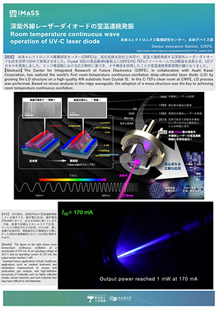
Research and development of UV-light emitting devices of nitride semiconductor
-
Visiting Associate Professor
YOSHIKAWA, Akira
Project
Research and development of thin film growth technology for wide band gap semiconductor devices

Surface/Interface
The materials used for power devices, solar batteries, LEDs, ceramics, and superconductors that help solve environmental and energy problems, as well as proteins required for drug development analysis, have crystal structures. By increasing our understanding and utilization of crystal growth, we aim to develop various materials that may change the world and produce materials that we have never encountered before.
Member
-
Project
Study on a novel processes based on crystal growth theory for high-quality crystal of functional materials (SiC, AlN, etc.)
-
Project
Application of information science to crystal engineering
-
Project
Control of defects in crystalline materials
-
Project
Thermal Control of Hybrid Hydrogen Storage by Absorption and Adsorption
-
-
Project
Evaluation Technology for Killer Defects in SiC Power Devices by Polarized Light Observation
-
-
Project
The development of an automatic defect inspection algorithm for semiconductor wafers
-
-
Visiting Professor
IZUNOME, Koji
-
Visiting Professor
UDA, Satoshi
-
Visiting Professor
KAMEI, Kazuhito
-
Visiting Professor
KOJIMA, Kazutoshi
-
Visiting Professor
SUZUKI, Atsushi
-
Visiting Professor
TSUKAMOTO, Katsuo
-
Visiting Professor
FURUSHO, Tomoaki
-
Visiting Professor
YONEZAWA, Yoshiyuki
-
Visiting Associate Professor
SEKI, Kazuaki
-
Visiting Associate Professor
MITANI, Takeshi
-
Visiting Faculty
KURASHIGE, Kazuhisa
-
Visiting Faculty
SUGIMOTO, Shuto
Nanomaterial devices
Member
-
Project
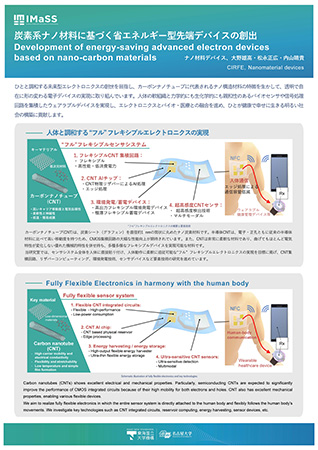
Development of energy-saving advanced electron devices based on nano-carbon materials
-
Project
Energy harvester based on nano carbon materials
-
-
-
Visiting Professor
KATAURA, Hiromichi
-
Visiting Faculty
OMACHI, Haruka
Energy Conversion Device
Member
-
Project
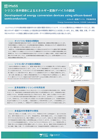
Advanced photovoltaic cells with earth-abundant materials
Advanced Device
Member
-
Project
GaN Power Devices
-
Project
GaN RF Devices
-
Project
Characterization of material properties of wide bandgap semiconductors
-
Visiting Professor
OSHIYAMA, Atsushi
-
Visiting Professor
OTOKI, Yohei
-
Project
Computational Studies on Semiconductor Crystal Growth
-
Visiting Professor
BOĆKOWSKI, Michał Stanisław
-
Visiting Professor
MIYAJIMA, Takao
Nanoelectronic Device
Member
-
Project
Research and development of thin film and interface engineering technologies of group-IV semiconductors for low-power consumption nanoelectronic devices
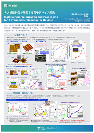
Semiconductor Engineering and Integration Science
Member
-
Project
Study on Materials Processing and Characterization for Advanced Electron Devices
Multiphysics Simulation Section
The Multiphysics Simulation Section is engaged in research with the aim of realizing multiphysical-system-based predictable crystal-growth simulations that integrate first-principles calculation with macroscopic fluid dynamics via thermodynamic analysis. Additionally,this section is pursuing proposals for new gallium-nitride-based power devices.
Frontier Computational Material Science
Crystal growth process clarified by the multi-physics simulation.
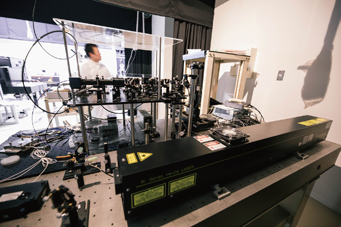
Materials Nano-Characterization Section
The Materials Nano-Characterization Section develops nanoscale operand analysis techniques for semiconductor devices under operating conditions using electron microscopy and electron holography.
These efforts are part of research centered on themes such as interface electronic properties involving direct measurement of device operations and electric-field response measurements for semiconductor interface electronic structures.
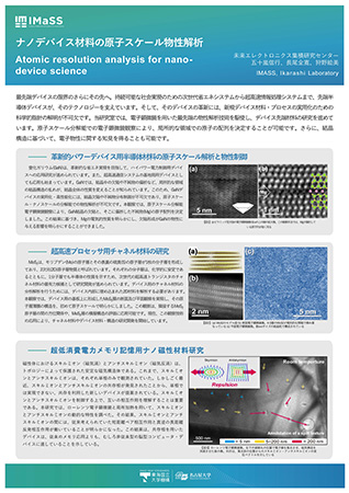
Nano-Electronic Materials (Ikarashi Lab.)
Nano-Electronic Materials
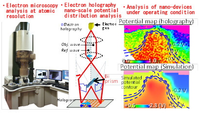
Direct electrostatic potential mapping in nano-scaled FET
under operation mode using electron holography
Member
-
Project
Nano-science and advanced electron microscopy for device innovation
-
Project
Analysis of Magnetic Properties by Advanced Electron Microscopy toward the Development of New Devices
-
Project
Advanced electron microscopy analysis of GaN and other nitride semiconductors
-
System Applications Section
In the area of devices utilizing cutting-edge electronics materials, this Section focuses on the integration of such devices into various systems and pursues applied research with an eye toward real-life applications throughout society.
-
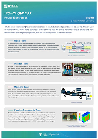
Power Electronics (Yamamoto Lab.)
-
RF Circuits (Hara Lab.)
Power Electronics
For the purpose of realizing high-efficiency, small, and lightweight power converters and motors used in hybrid vehicles, electric vehicles, power infrastructures, and next-generation airclafts, we carry out applied research on power electronics technology by integrating fields related to power semiconductors, controlling technology, and magnetic applications.
-
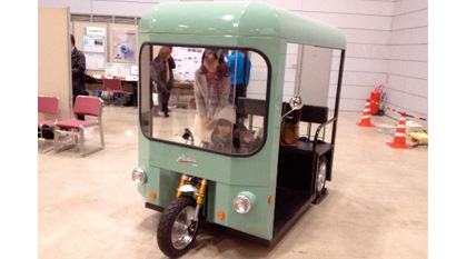
- Sightseeing electric vehicle developed in our laboratory (equipped with in-wheel motors, can be fully charged by capacitor charging in 4 min compared with 5 h using conventional batteries)
-
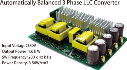
- Practical automobile power converter with highest power density in the world (3 W/cc or more) realized using GaN power semiconductor
Member
-
Project
GaN and SiC power semiconductor module techniques and its industry applications
-
-
Project
Research of advanced system simulation for Power Electronics and it's applications
-
-
Project
Research of high efficiency electric power conversion circuit using GaN Semiconductor Devices
-
Project
Development of Next-Generation Power Electronics Technology Based on Advanced Magnetic Application and Modeling Techniques and Its Industry Applications
-
Project
Study on electrical insulation for high-reliable and low-loss power semiconductor module
-

Project
Research of electronics packaging technologies for GaN and SiC power semiconductor module and its industry applications
-

-

-
Visiting Professor
ITO, Akira
-
Visiting Professor
UMETANI, Kazuhiro
-
Visiting Professor
SATO, Shinji
-
Visiting Professor
SHOYAMA, Masahito
-
Visiting Professor
CHIU, Huangjen
-
Visiting Professor
NISHIMURA, Kazunori
-
Visiting Professor
HOSOTANI, Tatsuya
-
Visiting Associate Professor
ISHIKURA, Yuki
-
Visiting Associate Professor
KURODA, Naotaka
-
Visiting Associate Professor
MASUZAWA, Takashi
-
Visiting Associate Professor
MASUDA, Mitsuru
-
Visiting Associate Professor
MUKAIYAMA, Daisaku
-

Visiting Associate Professor
MOSTAFA, Noah
-
Visiting Associate Professor
ANTOINE, Lesage- Landry
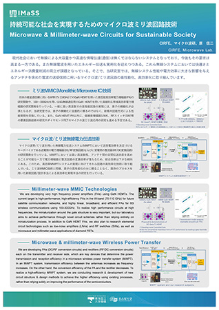
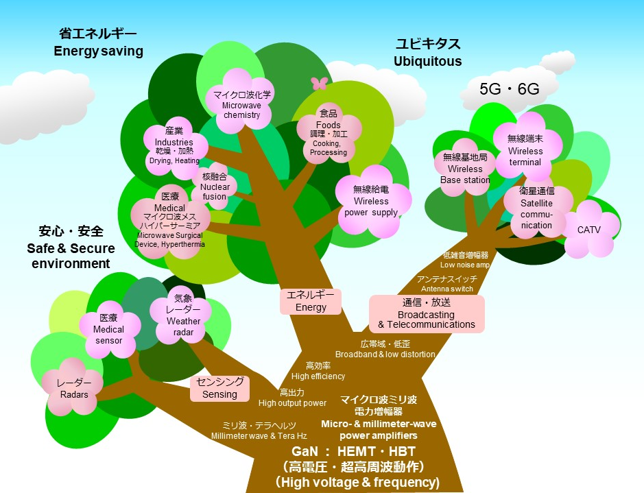
RF Circuits
RF circuits group conducts researches of new circuit technology and the basic performance improvement of the elementary devices, aiming for micro- and millimeter-wave applications such as wireless energy transfer, next generation wireless communication systems, etc. By taking full advantages of gallium nitride (GaN) devices, we aim to dramatically reduce the energy consumptions and contribute to the realization of the society coping both convenience and sustainability.
Member
-
Designated Professor
HARA, Shinji
Project
Circuit design technologies using GaN for microwave & millimeter-wave applications
-
Researcher
Kawamura, Hiroshi
Project
Circuit design technologies using GaN for microwave & millimeter-wave applications
-
Researcher
SAKUNO, Keiichi
Project
Circuit design technologies using GaN for microwave & millimeter-wave applications
-
Researcher
TANBA, Noriyuki
Project
Circuit design technologies using GaN for microwave & millimeter-wave applications
-
Visiting Associate Professor
Chung-Tse Michael Wu
-
Visiting Faculty
MIZOJIRI, Sei
International Research Section
The International Research Section engages in research and development activities together with visiting professors invited from overseas. Additionally, the Section is cultivating an international research network as part of efforts to form a central venue for nitride semiconductor research.
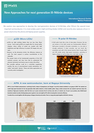
New Approaches on III-Nitrides (Pristovsek Lab.)
New Approaches on III-Nitrides
Future devices needs further III-Nitride semiconductor development, to go beyond the limits set by the current materials. New approaches like N-polar surface and new material like AlPN are explored which to achieve a device performance not possible using conventional approaches.
-
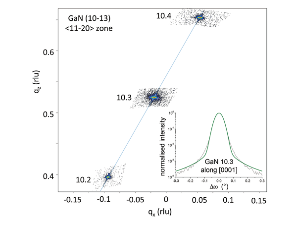
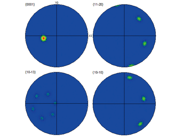
- Reciprocal space map using high-resolution X-ray diffraction to estimate the basal plane stacking fault density on (10-13) GaN crystals for green LEDs
-
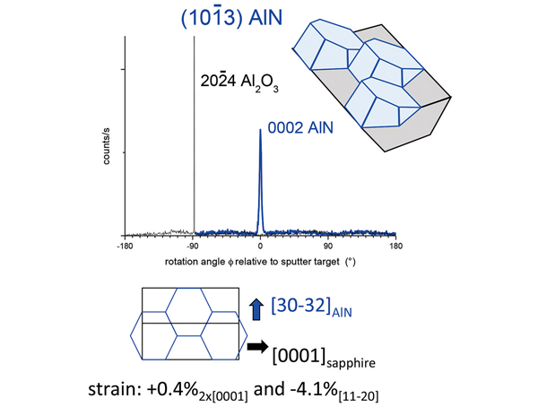
- Orientation of single phase (10-13) AlN on sapphire produced by directional sputtering and high-temperature annealing.
-
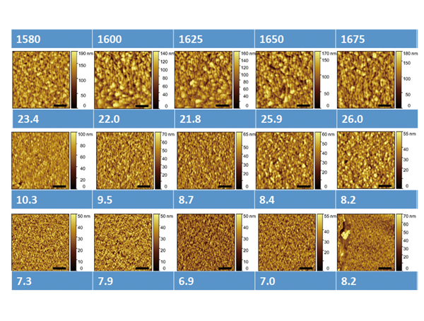
- Atomic force microscope images of (10-10) AlN films prepared by metal-organic vapour phase epitaxy with three different nucleation times and annealed at different temperatures. Numbers indicate roughness in nanometer.
Member
-
Project
Next generation of III-Nitride devices by a better understanding of crystal growth
-
Researcher
ROBIN, Yoann

Research Strategy and Joint Research Promotion Department
This organization was established to build a network as a co-creation platform for studying wide bandgap and ultra-wide bandgap semiconductor materials. And it is in charge of planning and managing projects to promote human resources exchange and joint research through the research network. This section is also provided a function secretariat of GaN research strategy office of Nagoya University.
Member
-

-
Designated Professor
UESUGI, Tsutomu
-
-
Designated Professor
TOMITA, Kazuyoshi
-
Designated Professor
NUNOUE, Shinya
-

Designated Professor
FUJITA, Shizuo
-
Designated Professor
YAGYU, Eiji
-
Visiting Professor
CHOWDHURY, Srabanti
-
Visiting Faculty
KORAI, Takao
-
-
-