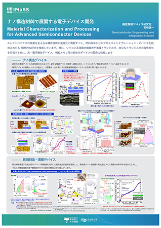
The Device Innovation Section aims to develop devices with new functions by establishing new crystal-growth methods and process development for cutting-edge electronics materials with a central focus onwide-bandgap semiconductors and ultrawide-bandgap semiconductors, such as gallium nitride, silicon cable, aluminum gallium nitride, and nanocarbon materials. A fully integrated research approach enables us to establish a unified process from crystal growth to device design, manufacturing, circuit dedign, and assessment.
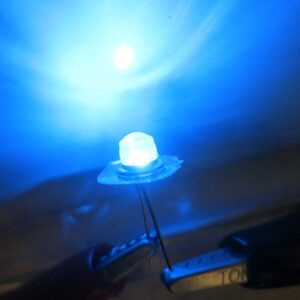
Prototype of Blue LED
-
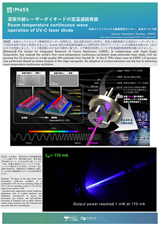
Crystal Growth (Amano Lab.)
-
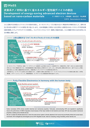
Nanomaterial devices (Ohno Lab.)
-
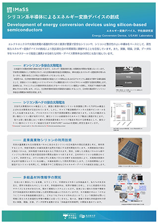
Energy Conversion Device (Usami Lab.)
-
Semiconductor Engineering And Integration-science (Miyazaki Lab.)