Research
Research Group
Interview with the staff of Koh Saitoh's Laboratory
Seeing nano in electron microscopy
With the development of innovative measurement techniques
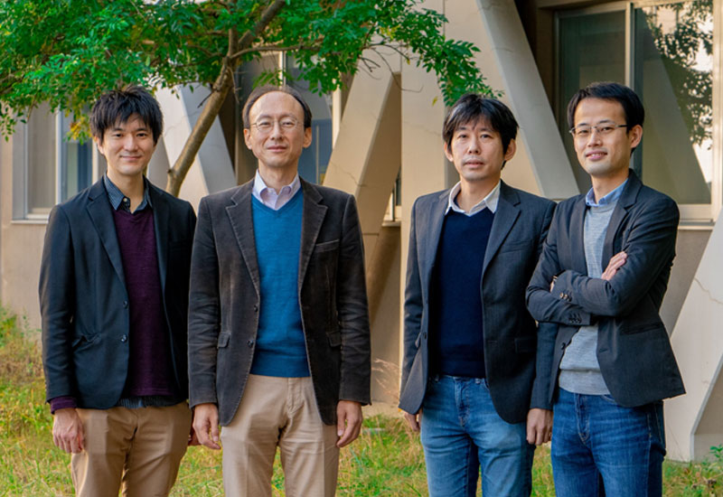
(Photo by Assistant Prof. T. Ishida at Research Laboratory Bldg.)
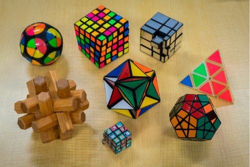
When you visit Saitoh's laboratory, you will find a number of beautiful but challenging 3D puzzles, such as wooden 3D puzzles and Rubik's Cubes with dodecahedrons. To solve these puzzles, you need a rich imagination, a variety of points of view, as well as meticulousness and tenacity. I feel that there is something in common with research, and feel as if I am being ushered into the philosophy of "beauty in mathematics". He sometimes uses them as an introduction to his students when he gives classes.
With innovative electron beams, the laboratory is developing equipment to show at the nanoscale physical phenomena that no one has yet seen.
What is the innovative electron beam? What kind of physical phenomena will it reveal?
Using an innovative electron beam
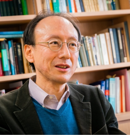
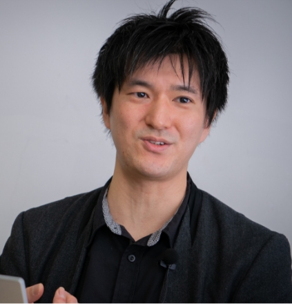
Professor
Koh Saitoh
profile
He studied physics at Tohoku University, where he obtained his Ph.D. in Physics for his research on the structural analysis of quasicrystals using electron microscopy. After working as a research assistant at the Institute of Multidisciplinary Research for Advanced Materials, Tohoku University, he was assigned to Nagoya University. Since he took his post at Nagoya University, he has been developing various electron microscopy techniques. Recently, he has been conducting fundamental research on new electron beams such as electron helical waves and their application to materials characterization methods.
● His pastime and hobbies: Puzzles, table tennis, classical music, mystery novels, and shogi recently
First of all, could you tell us what kind of research you are doing in Saitoh Lab?
Saitoh:We are developing innovative methods of using electron beams*1 to evaluate materials. One of them is spin-polarized electron microscope*2.Electrons are considered to spin like a top, with up-spin spinning upward and down-spin spinning downward. In an ordinary electron beam, they are mixed in a 50-50 ratio. However, the electron gun (i.e., the device that emits the electron beam) developed in our laboratory can emit electrons in either direction with 90% purity, making it the world's first transmission electron microscope that uses a polarized electron beam.
It's amazing to be the first in the world!
Saitoh:This electron gun is unique in the way it emits electron beams. Associate Professor Kuwahara has been studying this. He uses a phenomenon called the photoelectric effect*3in which electrons are emitted when light is shone on a semiconductor and it absorbs the energy of the light. By generating a pulsed electron beam, in which the electrons emitted are also pulsed when the light is pulsed*4it is possible to observe the phenomenon at the very moment the sample is irradiated.
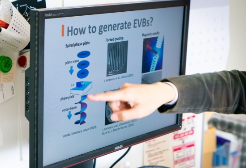
Another "innovation" is the electron helical wave. Electrons have the property of being waves, and their wavefronts are helical. This corresponds to orbital motion, and as with spin, I think its application to electron microscopy is an interesting idea.
The helical electron wave leads to the unknown, doesn't it?
Saitoh:When charged particles spin around like a vortex, they generate magnetism like an electromagnet, so we are conducting various researches on the idea that they might interact with magnetic materials, which are currently the focus of attention. We are also hoping that this beam can be used to sort out the chirality*5 of materials. This chirality separation is important for materials development.
Various methods of evaluation
What are some of the ways in which you evaluate things using electron microscopy?
Saitoh:There are three main ways. 1) Microscopy. The light of an optical microscope is converted into electrons, and an optical lens is converted into a magnetic field lens. 2) Diffractormetry*6. This is a method of inferring the arrangement of atoms from the characteristic patterns (diffraction patterns) created on a screen by electron waves scattered from a sample. 3) Spectroscopy. By analyzing the energy loss of the electron beam which interacts with samples, we can find…
So, you mean there's research into materials themselves, and there's also technology for identifying materials.
Saitoh:Most of the researchers who are involved in electron microscopy are studying materials (the things themselves). Many of them want to see materials, want to know materials, and electron microscopy is a tool for materials science. I am a researcher of electron microscopy techniques and do not research so much on the materials themselves. I look at the material as an application example to evaluate the performance of the technique.
Explanatory goods for "Diffraction".
When you look at a point of light through a thin mesh of fabric like organdy, a cross pattern appears. If you look closely, you can see that the rainbow is repeatedly lined up along the cross. The pattern does not change when the cloth is moved in parallel, but when the cloth is rotated, the crosses of light rotate with it. This is the same as diffraction in a crystal, where light waves scattered by the cloth's grain intensify in a particular direction. The rainbow appears because the direction of intensification differs depending on the wavelength. It is crystal structure analysis using diffraction that determines the pattern of the fabric based on the diffraction pattern of light.
Observe small, fast-moving objects.
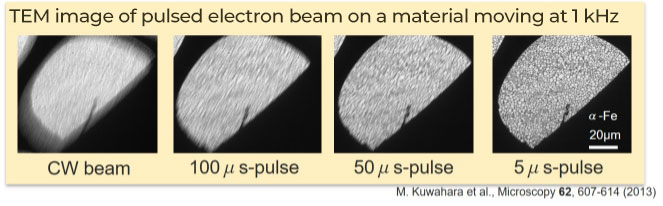
You have published " Development of Ultra Time-Resolved Electron Microscope Using Coherent*7 Ultrashort Pulsed*8 Electron Beams" on the web.

Kuwahara:With conventional electron microscopes, we can see things as small as atoms, but we can't see fast-moving objects because the image is blurred. But a microscope equipped with this analytical instrument can take pictures of every moving moment in succession at very high speed. This means that we can see, for example, how something moves from point A to point B, or how it degrades in a device, and it's also possible to photograph biological samples and polymeric materials.
Associate Professor
Makoto Kuwahara
profile
Born in Tokushima Prefecture, Japan. He received the Doctoral degree in the Department of Particle and Astrophysics at Nagoya University for his research on polarized electron sources for elementary particle experiments. After working as a postdoctoral fellow at Research Institute of Electrical Communication, Tohoku University, he was employed by Nagoya University. Since then, he has been developing new analytical methods using electron microscopy and applying them to advanced materials.
● His pastime and hobby: driving, traveling, movies
Wouldn't a biological sample be destroyed by an electron beam?
Kuwahara:Electron beams are very energetic, so when they hit the sample, the bonds are broken and the sample is destroyed, but with this microscope, we can take pictures of the sample before it is destroyed. Moreover, since it is safe to move, the sample does not need to be fixed, which is surprisingly time-consuming, so it is easier to use and has a higher industrial throughput.
When you talk about capturing things that are so small and moving that they cannot be seen, I feel as if you are talking about the subatomic particles of the universe that are expanding before my eyes. (hahaha).
Kuwahara:When I was a student at Nagoya University, I was in the physics department of the Faculty of Science, where we used accelerators to study subatomic particles (Nakanishi Lab), so I guess that's why I talk like that (hahaha). I was also interested in the field of quantum information, and for the next two years as a postdoctoral researcher, I worked on quantum repeaters and quantum communications at Tohoku University, but I came to my current laboratory when Professor Nobuo Tanaka, the predecessor of this laboratory, and Professor Nakanishi decided to collaborate. That's how I changed to this field, but all the experience I have gained so far has not been wasted.
I still want to design original equipment
Assistant Professor
Takafumi Ishida
profile
Born in Nagoya, Aichi Prefecture, Japan, he graduated from the Faculty of Science and Engineering at Meijo University in 2007 and completed his postgraduate studies there. He received his degree (Ph.D., Engineering) in the development of phase-contrast scanning electron microscopy at the Graduate School of Electronics and Information Systems, Nagoya University. After working as a postdoctoral researcher at EcoTopia Science Institute, Nagoya University, he was employed by the Institute for Future Materials and Systems, Nagoya University as an assistant professor in 2015.
● His pastime and hobby: Mainly indoor activities such as watching sports (ball games in general), movies and dramas, and sometimes driving.
Since baseball is out of season, these days he mostly watches videos on YouTube or Netflix, or drive.
Assistant Professor Ishida, are you also developing electron microscope equipment?
ISHIDA:Yes, just like Associate Professor Kuwahara, I am continuing my research to capture nano-scale phenomena, such as objects and materials that move too fast for the atomic-scale eye to follow. In particular, I am now motivated by the desire to capture the motions of new magnetic materials, such as skyrmions, or the state of the biological sample just before and the moment it is broken.
Are magnetic materials visible?
ISHIDA:Electrons are charged particles, so if there's a magnetic field on them, they bend under the force. By detecting the angle of the bend, we can measure the strength of the magnetic field.
That' s what you can do.
ISHIDA:We now have a microscope that allows us to see this directly, but it is very expensive, so we are continuing to develop another way to detect electrons with high sensitivity by applying the detectors of high-energy accelerators to solve the mysteries of the universe.
A Passion for the Search for "Amazing Substances".
Assistant Professor
Rikizo Yano
profile
Born and raised in Kawasaki City, Kanagawa Prefecture, he has been interested in robotics and electronics since a young age. At junior and senior high school, he immersed himself in club activities such as Go and table tennis, and at university, he joined Keio Table Tennis Team (Keio University Athletic Association), aiming to balance his studies with club activities. Realizing the importance of materials research in many fields, he went on to study at the Department of Innovative and Engineered Materials of Tokyo Institute of Technology, where he obtained his PhD (Science). Then, as a postdoctoral fellow, he conducted joint research at the National Institute of Advanced Industrial Science and Technology (AIST) and Nagoya University before taking up his current position in April 2008.
His pastime and hobby: Playing table tennis, Go, Kendama (Japanese cup and ball), Making crystals
Assistant Professor Yano, what kind of research are you doing?
Yano:In a word, I' m looking for "amazing substances". I am currently focusing on "topological materials*10, in which the "surface/interface*9"of a material and the material itself (the inner, non-surface part) have completely different properties. One example is there is the topological insulator, which has the properties of a metal with fast-responding electrons only on its surface, while the material itself is an insulator. Since these electrons are sensitive to magnets and magnetic fields, they are expected to be applied to highly sensitive magnetic sensors or extremely ultra-low-power-consumption devices that operate in micro-magnets.
Are there such electrons only on the surface of a material?
Yano:Yes, there are. Moreover, these surface electrons may be even more powerful. When a topological material is combined with a superconductor*11 it is believed that the same state as a yet-to-be-discovered particle called a "Majorana particle*12"appears at the interface, which is the junction part. Observing an undiscovered particle state is achievement in itself, but the Majorana particle is also expected to be used in quantum computers. They may be able to perform in a few minutes calculations that would take the supercomputer "Fugaku" tens of thousands of years.
If such "amazing substances" are discovered, what do you expect them to lead to?
Yano:It will change the world. For example, transparent materials such as glass and plastic bags do not normally conduct electricity. However, because human have found a material that conducts electricity even though it is transparent, we have been able to create things like touch panels for smart phones. Sometimes, a substance that looks ordinary at first glance can become an amazing substance or property when combined with another substance. Just like solar cells made by combining semiconductors and the Majorana particles*12 mentioned in the above example.
Pathways to Solution
I feel that the image of puzzles I have been familiar with since my childhood overlaps with the research that sheds light on the way to prove or solve a hypothesis with science. The research object that we want to know and understand is the behavior of electrons (subatomic particles).
Saitoh:Electrons are also subatomic particles, but they are everywhere, and the technology to extract them has been established. Moreover, they behave (move) exactly as we want them to according to certain equations. They do exactly what we set them to do, so we are using them to study the structure of crystals and materials, and then applying them to microscopes.
However, we are still investigating the fundamental properties of electrons some part of which we haven't learned yet. This may not lead directly to the development of materials immediately, but we never know what will happen.
Basic Knowledge
*1 Electron beam
An electron beam (EB) is a stream of high-velocity electrons emitted into a vacuum. Fluorescent lamps, television cathode ray tubes and X-ray tubes are devices that use electron beams.
*2 Spin polarization
The spin polarization is a spin-like property of electrons, which is also the source of magnets. There are two states of spin, upward (up/right-handed) and downward (down/left-handed), and a bias in either direction is called spin polarization.
*3 Photoelectric effect
A phenomenon in which electrons in a material fly out when light hits it. The electrons in a substance are bound by the gravitational pull of the atomic nucleus and cannot normally come out. In order to go out, energy is needed to break the bond. In the photoelectric effect, this binding is broken by the energy of light.
*4 Pulse
A general term for signals that change quickly and rapidly in a short period of time. An electric current or radio wave that flows for an extremely short time.
*5 Chirality
Chirality is a property of an object that prevents it from being superimposed on its mirror image. A shape with a difference between left and right is called chiral, and the human hand is a typical example of chiral. Some molecules have the same molecular formula, but their steric structures are mirror images of each other, and some have completely different chemical properties. For example, in thalidomide, the right-hand system (R-body) works as a sleeping pill, while the left-hand system (S-body) is a compound with strong teratogenic properties. It is important to develop a method to quickly and accurately separate the chirality of these substances. Incidentally, Professor Emeritus Yoshio Okamoto of Nagoya University (former visiting professor at Ecotopia Science Institute) received the "Japan International Prize" for his great contribution to the basic development of separation reactions, and Special Professor Ryoji Noyori was awarded a "Nobel Prize" for leading the world in reaction development.
*6 Diffraction
A phenomenon in which a traveling wave travels around such a shadowed area as behind an obstacle. For example, a sound can be heard even when it is behind an object. This phenomenon is called diffraction. The larger the wavelength relative to the obstacle, the larger the diffraction angle.
*7 Coherent
It is a term used to describe the tendency of waves to interfere with each other, meaning that there is a constant relationship between the amplitude and the phase of two or more waves. It is similar to rhythm in music. Laser light is a highly coherent light and is sometimes called coherent light.
*8 Ultra-short pulse
An ultrashort pulse is a signal that has a rapid amplitude (wave) in an ultra-short time period of a few femtoseconds to a few picoseconds. 1 femtosecond = 1 fs = 1 x 10-15 sec = 1/1000 trillion 1 picosecond = 1 ps = 1 x 10-12 sec = 1/1 trillion Incidentally, even light, which travels at a speed of about 300,000 km per second (a distance of seven and a half times the circumference of the earth), travels only about 0.3 µm in one femtosecond. The distance travelled by light in a femtosecond is about 0.3 μm.
*9 Interface
It is the point at the boundary between two neighboring substances.; the boundary where two substances are joined.
*10 Topological substances
Topological substances are a group of substances discovered using the mathematical concept of topology, which classifies substances by the number of holes they have. Many different types of substances have been found. The contents of a substance (its bulk) can be studied to reveal the strong properties of its surfaces and interfaces. A typical example is topological insulators, which are insulators but have fast-moving Dirac electrons (electrons that move at high speed through the material as particles that appear to have no mass) on their surfaces, and are attracting attention as next-generation semiconductor materials.
*11 Superconductors
A material that exhibits a quantum phenomenon in which electrical resistance suddenly drops to zero when cooled below a certain temperature, which varies depending on the material. Superconductors have practical features such as the ability to transmit electricity with zero loss and the ability to create a strong magnetic field.
*12 Majorana particle
The Majorana particle is defined as the antiparticle of itself, and it has recently been shown that the same state as the Majorana particle can appear in matter (in a special superconducting state). If the existence of this particle is confirmed, it would be possible to control the state of the Majorana particle by simply replacing it, thus creating an unprecedented quantum computer of the braided type. Therefore, there are high expectations for this "usable subatomic particle," and it is considered important from both the perspective of basic physics and applications, and the world is continuing to challenge its existence.
Text extracted from "IMaSS NEWS Vol. 10" Special Issue, IMaSS Publicity Committee (T. Miwa and M. Konishi)
[English translation by J. C. Oates]