IACC
Organization
Industry–Academia
Collaborative Chair
 Section / Group
- MIRISE Technologies Advanced Power Electronics Industry-Academia Collaborative Chair
- TOYODA-GOSEI Leading Innovative R&D Industry-Academia Collaborative Chair
- AsahiKASEI Innovative Devices Industry-Academia Collaborative Chair
- TOYOTA CENTRAL R&D LABS GaN Power Device Industry-Academia Collaborative Chair
- MITSUBISHI CHEMICAL GaN Substrate Devices Industry-Academia Collaborative Chair
- Photo electron Soul / Nagoya University, Joint Lab. of GaN e-beam Device
- UJ-Crystal ultra-high quality SiC IA Collaborative Chair
- Aixtal Semiconductor Process Informatics Industry-Academia Collaborative Chair
- D4 Atomic Layer Engineering Industry-Academia Collaborative Chair
- NGK Advanced Nanomaterials Industry-Academia Collaborative Chair
- Fujitsu-Nagoya University Advanced Materials Application Technology Industry-Academia Collaborative Chair
MIRISE Technologies Advanced Power Electronics Industry-Academia Collaborative Chair
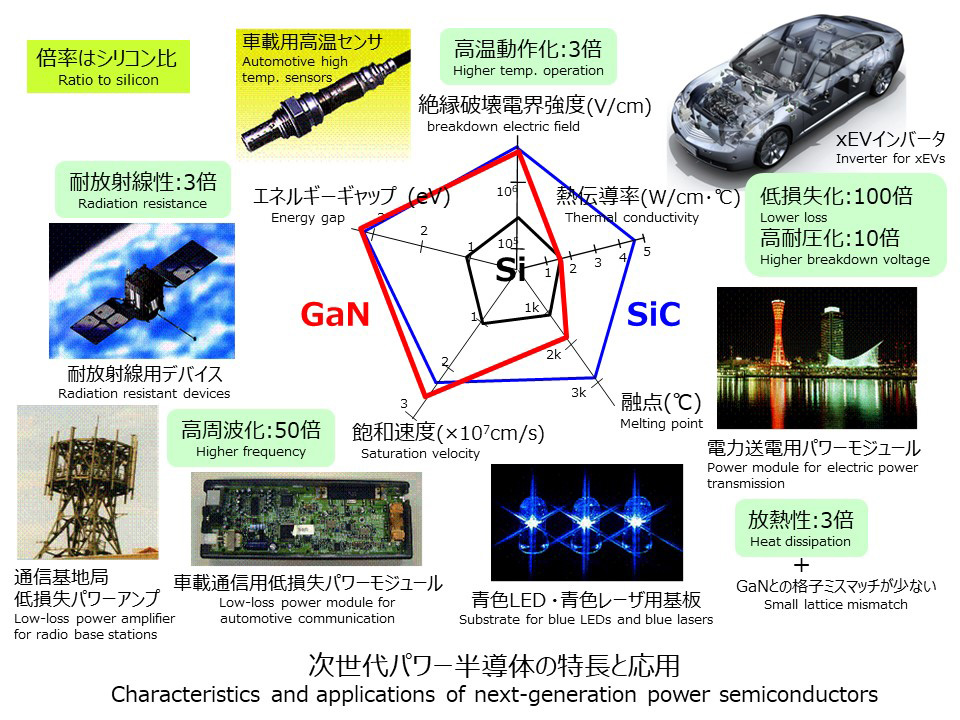
MIRISE Technologies Advanced Power Electronics Industry-Academia Collaborative Chair is looking into the future of high-power, high-efficiency, and high-frequency electric drive systems for electrification vehicles, and promoting exploratory research into gallium nitride power semiconductor materials, devices, and application systems.
Member
-
Designated Professor
ONDA, Shoichi
Project
Development of Crystal growth of the next-generation power-semiconductor materials
-
Project
Research of quality improvements and cost-reduced technologies of the next-generation power semiconductor crystals
-

Project
Research of Fabrication Process and Device Structure of GaN Power Devices
-
Project
Research on Low-Cost Manufacturing Process Technologies for GaN Power Devices
-
Project
GaN power device structure, fabrication process, and practical research
-

Project
Research of Fabrication Process and Device Structure of GaN Power Devices
TOYODA-GOSEI Leading Innovative R&D Industry-Academia Collaborative Chair
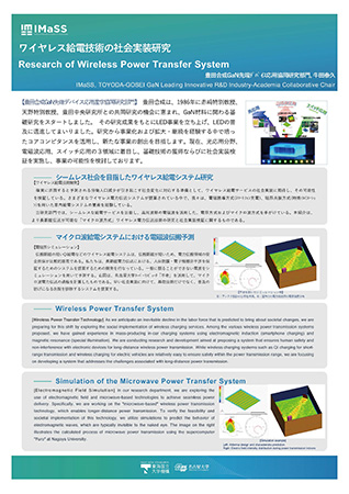
TOYODA-GOSEI Leading Innovative R&D Industry-Academia Collaborative Chair
In 1986, Toyoda Gosei Co., Ltd., started a joint research project with Professor Akasaki, Professor Amano, and Toyota Central R&D Labs., Inc., and began fundamental research on GaN materials. The commercialization of LEDs and their subsequent widespread adoption were based on this research. The core competencies cultivated from research, commercialization, expansion, and continuation will be utilized to create new business opportunities.
Member
-

Project
Research on characteristic analysis and modeling of GaN power devices
-
Project
Advancement of elemental technologies for GaN-based devices
-

Visiting Professor
FUKUSHIMA, Hideoki
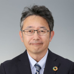
AsahiKASEI Innovative Devices Industry-Academia Collaborative Chair
AsahiKASEI Innovative Devices IA Collaborative Chair exploit our high-quality AlN single-crystal substrate technology, exploratory research into novel devices, and applications to create new business opportunities.
AsahiKASEI Innovative Devices Industry-Academia Collaborative Chair
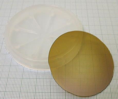

TOYOTA CENTRAL R&D LABS GaN Power Device Industry-Academia Collaborative Chair
TOYOTA CENTRAL R&D LABS GaN Power Device Industry-Academia Collaborative Chair
In order to realize GaN power devices, we research the following:
①Epitaxial growth with precise control of impurities and point defects
②Gate insulators and MOS interfaces
③Process technologies, such as low-damage etching and ion implantation
④Device design for very low loss
-
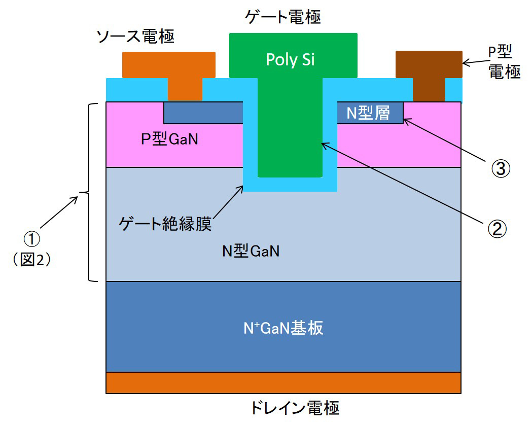
- Fig.1 A Vertical trench GaN device
-
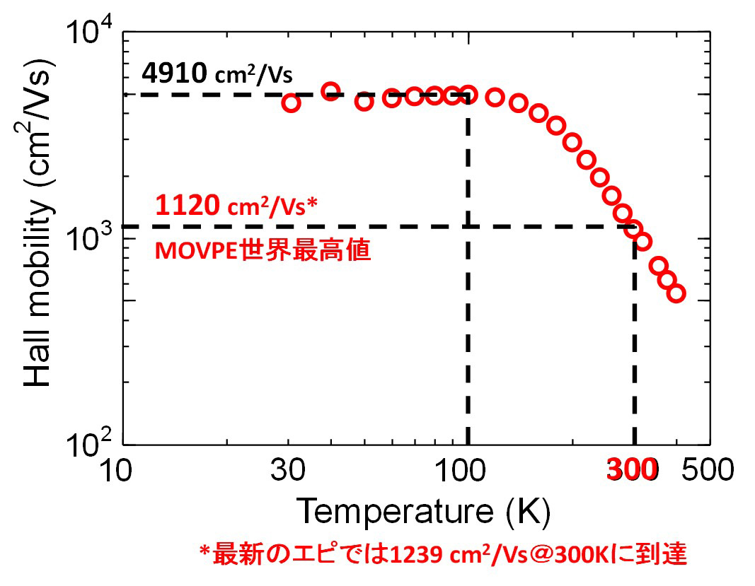
- Fig.2 Hall mobility in our n-type low-doping epi-layer
Member
-
-

Project
Process technology and device design and evaluation for GaN power devices
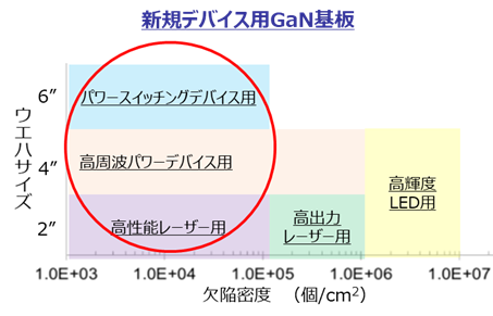
MITSUBISHI CHEMICAL GaN Substrate Devices Industry-Academia Collaborative Chair
MITSUBISHI CHEMICAL GaN Substrate Devices Industry-Academia Collaborative Chair
MITSUBISHI CHEMICAL GaN Substrate Devices Industry-Academia Collaborative Chair is engaged in the research and development of high-quality gallium nitride (GaN) substrates that serve as the foundation of new device structures exploiting the excellent properties of GaN, focusing on the following themes.
・Investigation of the correlation between substrate quality (e.g., crystal defects, impurities) and device characteristics, as well as elucidation of the mechanism underlying the correlation
・Clarification of the quality and characteristics required for GaN substrates for new devices
Member
-

-
Project
Research and development of high-quality GaN substrates for high-performance semiconductor devices
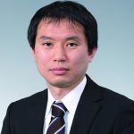
Photo electron Soul / Nagoya University, Joint Lab. of GaN e-beam Device
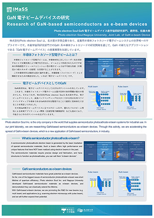
Photo electron Soul / Nagoya University, Joint Lab. of GaN e-beam Device
Photo electron Soul Inc. is the only one company in the world that supplies semiconductor photocathode e-beam systems for industrial use. With Nagoya University, in this joint laboratory, we are researching GaN-based semiconductors as e-beam devices. Through this activity, we are accelerating the industrial usage of “GaN e-beam devices”, which is a new application of GaN-based semiconductors.
Member
-
Project
R&D of GaN-based semiconductors as e-beam devices

UJ-Crystal ultra-high quality SiC IA Collaborative Chair
UJ-Crystal Co., Ltd. is a venture company originating from Nagoya University, and aims to quickly implement in society of ultra-high quality SiC single crystal substrates using the SiC solution growth technology and machine learning technology cultivated. This will enable further energy savings in the EV and smart grid fields and contribute to carbon neutrality.
Member
-
Project
Research on solution-growth technology for high-quality SiC crystals

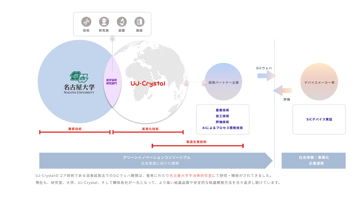
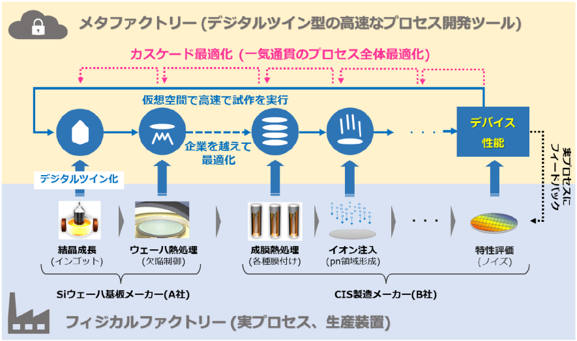
Aixtal Semiconductor Process Informatics Industry-Academia Collaborative Chair
Aixtal Corporation is a Nagoya University startup that aims to optimize the semiconductor manufacturing process across corporate boundaries by building a "semiconductor meta-factory" involving the entire semiconductor industry using process informatics (PI) cultivated through the development of SiC crystal growth processes.
Member
-
Designated Professor
MAEDA, Susumu
-
-

Visiting Associate Professor
TAKAISHI, Masaki
D4 Atomic Layer Engineering Industry-Academia Collaborative Chair
The D4 Atomic Layer Engineering Industry-Academia Collaborative Chair focuses on developing atomically engineered thin-film and interfacial materials, including inorganic nanosheets. Through these e orts, the chair aims to enhance catalytic functions and contribute to applications in next-generation electronic devices, environmental technologies, and energy-related fields. The chair also pursues the development of novel nanostructures.
Member
-

Designated Associate Professor
NAKAMURA, Maki
Project
Energy Applications of 2D Nanosheets
-

Designated Assistant Professor
MORITA, Shu
Project
Development of novel nanosheets and their application to electronic materials
-

Visiting Professor
ASADA, Ken
Project
Development of Nanosheet Applications
NGK Advanced Nanomaterials Industry-Academia Collaborative Chair
NGK Advanced Nanomaterials Industry -Academia Collaborative Chair promotes advanced research centered on the development and application of inorganic nanomaterials, with the aim of creating new products and businesses that contribute to the realization of a carbon_neutral and digital society.
Member
-
Project
Synthesis and applications of inorganic nanomaterials
-

Project
Synthesis and applications of inorganic nanomaterials
-

Project
Synthesis and applications of inorganic nanomaterials
-

Project
Synthesis and applications of inorganic nanomaterials
Fujitsu-Nagoya University Advanced Materials Application Technology Industry-Academia Collaborative Chair
Member
-
-
Project
Creation of Next-Generation GaN Power Devices