Research
Research Group
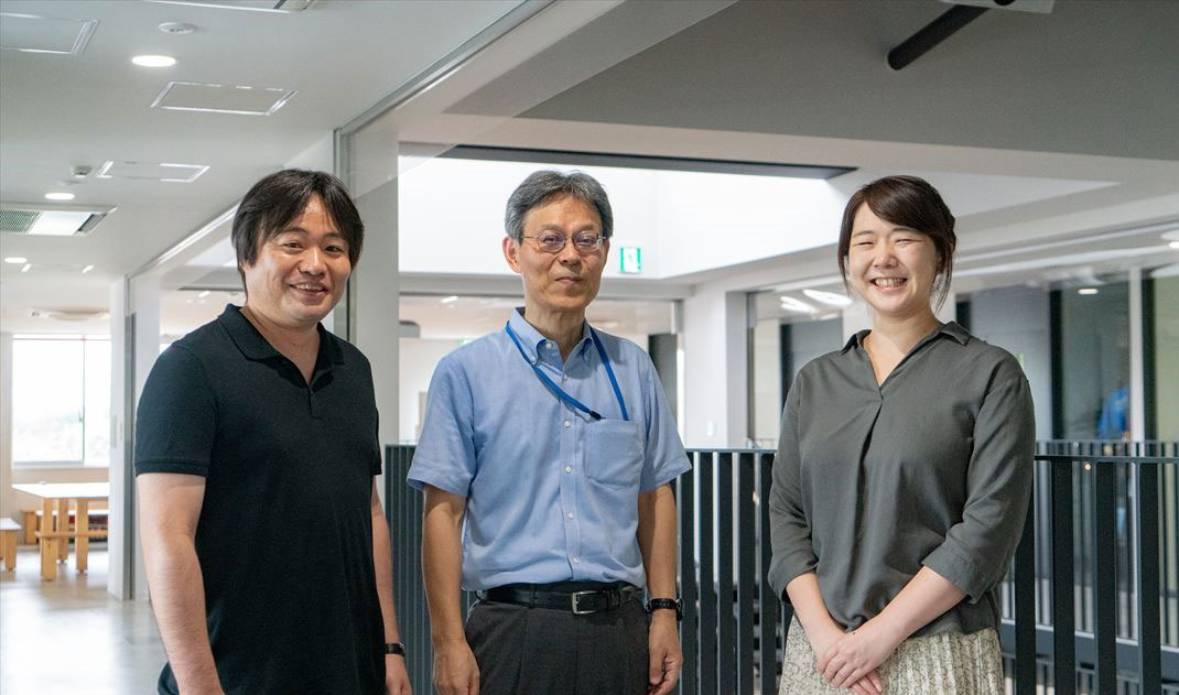
The interview with the staff of Ikarashi's Lab.
A breakthrough has come in technological innovation!
The discovery of mystery carves out our future.
There are a variety of IC cards, which we think are used by everyone now; such as "manaka" (prepaid smartcards used for transportation), credit cards, staff ID cards, student ID cards. They are called ID cards, because integrated circuits are used inside and outside. That means the thin cards are full of electronic parts such as resistors, capacitors, transistors. Electrons move at ultrahigh speed and stop suddenly because of electromagnetic induction and microwaves, and transmit an incalculable number of signals accurately in a moment. Have you ever asked how these devices have become so small and thin? Have you asked what they look like and how large they were some years ago?
Semiconductors have made remarkable developments because of a number of technological innovations. In the innovations, the activities of Ikarashi's Laboratory are outstanding. We have asked what is the semiconductor, which we don't usually see in our life and which has been developing so quickly that a lot of people find them puzzling, and have also asked about what they do in their research.
Analyzing the structure and properties of matter.
To begin with let us know what researches you conduct in Ikarashi's Lab.
Ikarashi:What we aim at in the Labo. is analyzing the structure and properties of matter such as semiconductors on the basis of cutting-edge science for innovation. The Electron Microscope is the main tool we use for analyzing them at nanometer.
Professor
Nobuyuki Ikarashi
profile
In 1988 he received his master's degree of Physics at Graduate School, Division of Science and Engineering of Tokyo Institute of Technology. He was employed by NEC Corporation and later by Renesas Electronics Corporation. Since 2015, he had been Professor of EcoTopia Science Institute, and since the institute was renamed, he has been Professor of IMaSS.
● He likes cooking and tasting the food. He sympathizes with the author of "Dan-style cooking," who says in the book, "Nothing else pleases me on the earth than going shopping for cooking." He also likes mountain climbing, though he has had no chances to do so recently. He also likes playing soccer and watching the games. He confesses that he has not applied himself to training at all recently.
Will you explain to us about such terms as "nanoscale*1" and "semiconductor" so that we can get a better idea of your researches?
Ikarashi: In the world, semiconductor devices such as semiconductor elements and integrated circuits are used in every part of daily life. They are used in electric appliances such as television sets, personal computers, smartphones, air conditioners, and also in automobiles and IC cards. At the end of the 20th century, most of them were nano-sized. We know that slight deviations or differences in the arrangement of molecules and atoms (crystals) in the materials themselves can significantly change their performance.(About semiconductor devices, let me explain in more detail later.)
You mean that in the semiconductor industry, of which there is world competition for control, what you deal with is the design and manufacture of components that are too small to be seen by the human eye.
Ikarashi:The smaller the semiconductors are, the less material we need for them and the less they cost. The distance the electrons move becomes shorter, and the treatment finishes faster, and less electricity is consumed. Now, however, we are working on important researches to integrate further; how it will be possible to make heat radiation less (reduce the loss of energy), and how we can get rid of the disorder of the crystal arrangement of the material itself.
I hear that you're trying to find the cause of such problems in order to solve them. May we ask how?
Ikarashi:Suppose there's malfunction that prevents electricity from running as we expect. Since the device is invisible to the naked eye, it's not too much to say that the electron microscope is the only thing we can depend on to find out where the cause lies. The electron microscope shows what the problem is, pinpointing the place.
What is the semiconductor device?
Will you tell us more in detail about the semiconductor device you mentioned?
Ikarashi:To begin with, the device is what was designed to do a particular job. I think I can say it is a combination of electronic parts or equipment. There are a variety of devices including personal computers, mouses, keyboards, printers. CPU, memory, hard disks, disk drives are also devices. The use of semiconductors for the materials makes it possible to turn lots of dreams into reality.
Semiconductors conduct electricity in particular conditions. Conductors like metals conduct electricity all the time. Insulators don't conduct electricity at all. That is what we learned at school.
Ikarashi:That's right. People used to connect a metal or a copper wire to send an electric current to something and switch on or off by hand. Now, we use semiconductors. No electricity flows if nothing is done, but suppose we use semiconductors in a circuit or in a board. They conduct electricity the moment they enter an electric or magnetic field, and it is possible to convey information or write in an electronic medium in an instant without doing anything by hand. It is also possible to stop it in the same way.
That is why you are engaged in developing the power device and the like by using GaN*2 , which has great potential to achieve as a semiconductor. Isn't it?
Ikarashi:We have a dream of contributing more to the society by using GaN to produce devices that can withstand heavy current and high voltage. We are trying very hard day and night to contribute to the development of new technology by analyzing the physical properties mainly with the electron microscope wondering which is the best mixed material to use as a device and how it can be done.
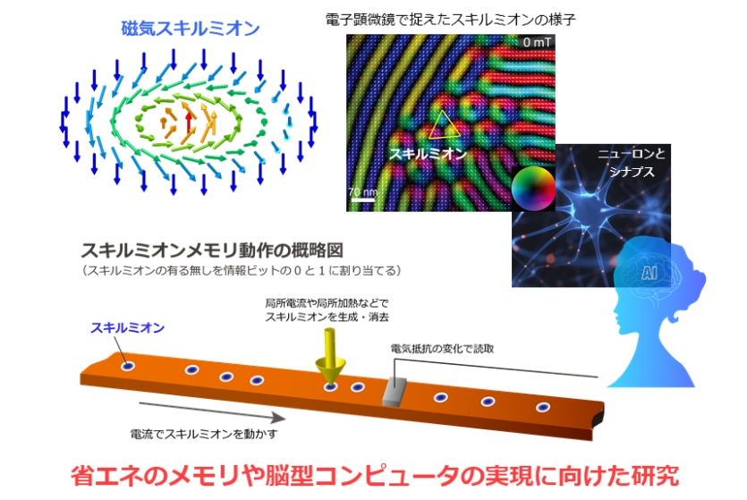
Trying to analyze magnetic skyrmions, which will serve amazingly as energy-saving technology.
Associate Professor
Masahiro Nagao
profile
In 2008, he completed the Ph.D. program at the Graduate School of Science and Engineering of Waseda University. In the same year, he was employed as doctoral research fellow at National Institute for materials and science (Independent Administrative Corporation). In 2012, he became Assistant Professor at the Graduate School of Science and Engineering of Waseda University. In 2016 he was employed as Associate Professor at IMaSS. He is now engaged in the development and application of physical characteristics of topological materials with the Transmission Electron Microscope.
● His pastime: He likes to send healing cat videos to his students.
Associate Professor Nagao, is the analysis of semiconductors your main research?
Nagao:My research is mainly on magnetic materials, the materials for magnets. Now I am analyzing magnetic skyrmions particularly. Skyrmions are a tiny vortex that have the characteristic of looking like particles, which was originally the concept of nuclear physics developed by Tony Skyrme, a British physicist. In 2010, it was discovered that the particles were also in magnets and that they moved when electricity flew. Topology*3 is a branch of mathematics, and the research on skyrmions has a lot to do with Topology,
What is expected of the research on skyrmions?
Nagao:Something having the property of topology moves with the minimum amount of electric current. I number 0 or 1 depending whether it has skyrmions or not. I hope that I can produce more energy-efficient electronic devices or memory. Recently the research of producing a device that mimics the human brain has been published. The world keeps watching the research of skyrmions. They have the merit that they can be observed with the electron microscope. With great interest, I have been conducting the research since 2013.
Did you want to be a researcher in your childhood? Is there anything you are good at?
Nagao: Little did I dream of becoming a researcher. I just wanted to go to university, but had to spend one more year preparing for university. I didn't care which department to choose before I got into Waseda University. As a student at Waseda, I didn't even know about graduate school. What I'm good at is playing the piano. I started it as a little boy and kept practicing it. I had wanted to be a jazz pianist until sometime at high school.
Do you think there is anything common both to music and research?
Nagao:As for music, it sounds quite different if played in a different way. That is what research shares in common with music. The research with the same results may give different information. We may present the result in a different way from others, and those who listen to them may accept them in a different way. A research paper is a kind of work showing what the person feels and wants to communicate. That is what is common to music.
The first person in the world to see this!
Assistant Professor Kano, I hear you took up your new post in April. What do you think is the attraction of electron microscopy?
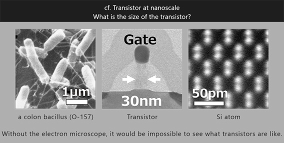
Kano:I used to conduct researches on graphene*4, the ultimate 2D material, and used the transmission electron microscope (TEM). I magnified 1,000 times or one million times depending on what I observed. Anyhow what we cannot see with our naked eye at all when it exists there appears before our eyes through TEM. What was quite invisible becomes visible. I saw each atom of the 2nm carbon nanotube. That made a strong impression on me. It struck me at that time that I might be the first person in the world to see it. I think it is the attraction of electron microscopy.
Assistant Professor
Emi Kano
● Her hobby: Singing songs. Since she started singing in chorus at junior high school, she has been doing so, even after graduation.
What do you want to say to senior high school students?
Ikarashi:I want them to keep on asking what they like to do. They can graduate from university with a diploma if they fulfill the requirements, but there'd be no attraction in life if they had nothing they want to do. As they do lots of things, they may often experience what they will regret later. When they're at university, they can waste time and money. What I want them to do is find what they want to do, to find the field in which they can think of better and more interesting ways to do things.
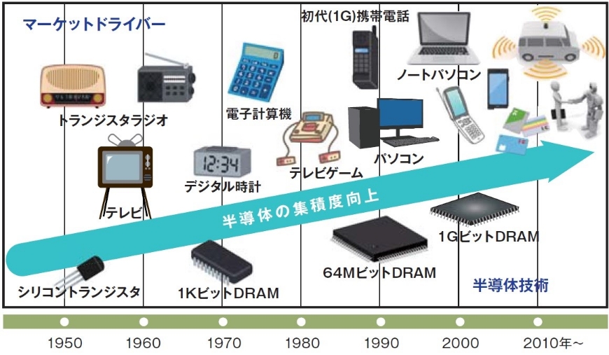
The computer with vacuum tubes in it was developed in 1946 (ENIAC), and it weighed about 30 tons. It was the largest electronic machine in the world, which had about 18,000 vacuum tubes in it. The about 160m2 building was full of vacuum tubes (used for amplifying electricity), and the power consumption and the heat generation were gigantic. The circuit primes were about 110,000 in total.
Later, the electronics industry stared to change with the study of semiconductors and the development of transistors (used for amplifying electricity.)
In 1959, IC (integrated circuit) was invented, and in the world including Japan, there was a severe production competition of electronic calculators until the end of the 1970's.
In 1965, the Moore's law proposed by G. Moore of Intel Corporation said that the accumulation density of large-Scale Integration would be twice as high in one and a half years, four times as high in three years, and 1,000 times as high in 15 years, and in fact, what was said had happened and has been happening even now.
Later, IC developed dramatically into LSI, and in the 1980's, developed into VLSI (whose accumulation density is as high as 100,000 to 10,000,000), and in the 1990's, developed into ULSI (whose accumulation density is as high as more than 10,000,000.) The technological innovation was so radical.
In the 2000's, the production of system LSI (LSI having ultra multi-function on a single chip) started at full swing. It has been applied in such a variety of fields that semiconductors have been used in every part of our society and support our life,
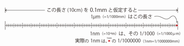
*1 nanoscale
A size that can be measured in nanometers (a.k.a. nanometer-order.)
1nm=10-9m=0.000000001m 1 millionth of 1mm
*2 GaN
Gallium nitride. It is a nitride of gallium. It is a semiconductor used as the material for blue LED, for which Professor Amano at IMaSS was awarded a Nobel Prize. In recent years, it has been expected that the semiconductor will be applied as power semiconductor or to a radar.
*3 topology
Homeomorphism, geometry studying geometric properties kept after translation, rotation, inversion, enlargement, reduction. The term made up of "topo" (Greek word meaning location) and logy (meaning study.)
*4 graphene
Substance in which Carbon atoms are put together in a hexagonal pattern like a honeycomb.It is as thick as an atom. It is light and superior to anything else in its tensile strength and thermal conductivity. It is the ultimate 2D material that moves electrons faster than anything else at room temperature. It is almost translucent and is the ideal material for touch screens and solar batteries. It is expected as a new generation semiconductor.
Text extracted from "IMaSS NEWS Vol. 09" Special Issue, IMaSS Publicity Committee (T. Miwa and M. Konishi)
[English translation by Shozo Ikuta]