Research
Research Group
Amano Laboratory: Interview with young researchers
Pursuing GaN research in the hope of a better life for future generations
Message from Professor Amano
Gallium nitride (GaN) has attracted much attention as the material of blue light-emitting diodes (LEDs). However, its potential application is not limited to light-emitting devices. If GaN can be used as the material of power devices, a further reduction in power consumption of ~10% in addition to the 7% brought about through the use of LED bulbs may be expected. There are 48 nuclear power plants in Japan, as of 2016. The amount of energy that could be saved through the use of LEDs and power devices accounts for approximately half the energy generated by all nuclear power plants.
Three up-and-coming young researchers, Dr. Honda, Dr. Nitta, and Dr. Deki, have been tirelessly performing research so that GaN may be applied to devices that can be used in society, along with postdoctoral researchers and students of my laboratory. They are truly enthusiastic and delightful researchers. Please come to my laboratory and visit them.
Professor Hiroshi Amano, Director of the Center for Integrated Research of Future Electronics (CIRFE)
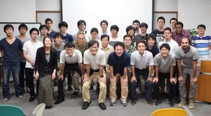
(third from the left in the front row in the top-right photo)
Addressing challenging problems with flexible ideas and fresh viewpoints
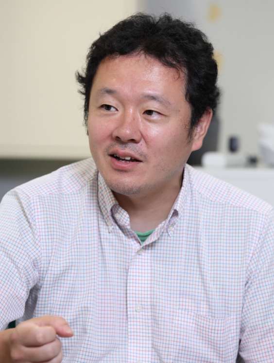
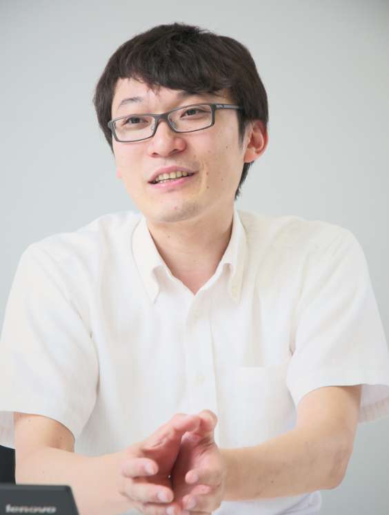
Dr. Yoshio Honda, associate professor
・Specialties: electronics and electric material engineering
・Hobbies: spending time with family, going out drinking, skiing
What kind of research are you involved in at Amano Laboratory?
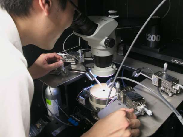
Dr. Honda:I’m involved in a wide range of research from materials to devices based on GaN. In particular, my main interest is the development of power devices. Power devices are used for power conversion and control. The loss of power associated with the power conversion and control of GaN devices is much smaller than that in currently used silicon (Si) devices. Therefore, GaN devices can realize high efficiency and performance.
The members of Amano Laboratory are involved in a wide range of research. Please describe to us the research organization of the laboratory.
Dr. Nitta:Some faculty members, such as Professor Amano and Dr. Honda, have devoted their whole career to research in the university and play a central role in the laboratory, while other faculty members, including myself, have experience working in companies. I believe that the current research organization is ideal for realizing timely and academic research that is beneficial to society by pursuing research from both scientific and manufacturing viewpoints.
Addressing research that will expand the potential of nitride semiconductors
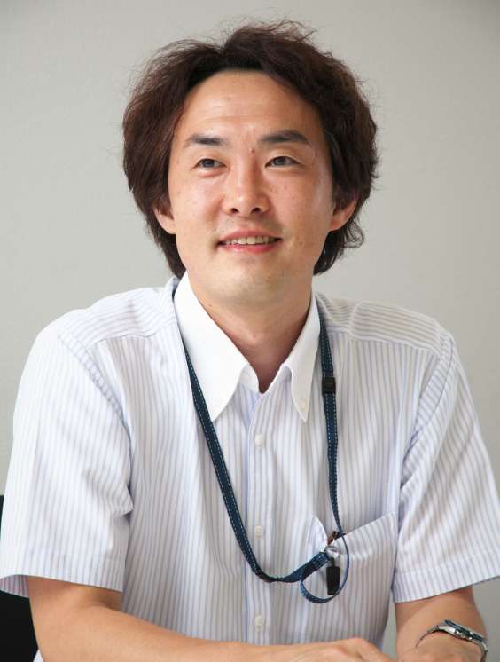
Dr. Shugo Nitta, specially appointed associate professor
・Specialties: crystal growth, device engineering
・Hobbies: spending time with his children, futsal
Describe the atmosphere of Amano Laboratory?
Dr. Deki:In terms of research, researchers of silicon carbide (SiC) power devices, in addition to GaN specialists, have joined the laboratory, bringing fresh perspectives to the laboratory. Students are also enjoying an environment where they can experience a wide range of research themes from the crystal growth of GaN to the fabrication of power devices. The laboratory is really active.
Dr. Honda has been at Nagoya University for 22 years since entering Nagoya University as an undergraduate student. What did you study when you were a student?
Dr. Honda:When I was a student, I grew GaN on silicon substrates. I was originally interested in semiconductors when I was an undergraduate student and I selected Amano Laboratory because it was involved in research on semiconductors. The laboratory was focused on GaN then, a material that I was unfamiliar with. I was interested in this blue-light-emitting GaN. At that time, researchers had only grown GaN on sapphire substrates. Therefore, I wanted to investigate the challenging idea of growing GaN on a Si substrate until I received my Ph.D. degree. Ever since then, my policy has been to try doing things that no one has ever done. Growing GaN on Si substrates is part of this.
Looking at evaluation to achieve the reliability necessary to market products
Dr. Manato Deki, assistant professor
・Specialties: electronic devices, electronics material engineering
・Hobbies: Shogi, the frame trap in the “Street Fighter” video game
Dr. Nitta has had experience working in a company. Please tell us about your previous difficulties in research and your role in the laboratory.
Dr. Nitta:The primary purpose of the research and development carried out at companies is to realize a required performance. To market products, the specifications of a product need to be indicated on design drawings. I found it difficult to become accustomed to this process. For mass production, rather than to realize the highest performance of a product, we must look at how to guarantee a reliable performance. I realized that different priorities are required in the fields of research and manufacturing. I think one of my roles in the laboratory is to narrow the gap between different viewpoints and experiences, such as the gap between faculty members and students, the gap between inside and outside of the laboratory, and the gap between academia and industry.
Dr. Deki is looking at evaluation to improve the reliability of devices. The efficiency of devices seems to be dependent on the type of material.
Dr. Deki:For example, for the power conversion carried out in bullet trains and electric vehicles, changing the material used in power devices can reduce the power loss during switching, leading to a ~10% increase in power conversion/fuel efficiency. In another example, when the thermal conductivity of a material used in car engines is poor, a system to distribute cooling water is required, which decreases the overall efficiency because of the increased weight of the car. Because GaN and SiC have higher thermal conductivities than Si, air cooling instead of water cooling can be adopted. Therefore, the entire system can be downsized and the fuel efficiency will increase.
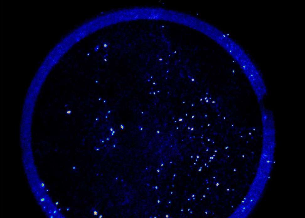
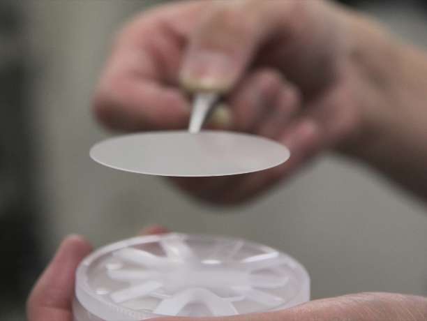
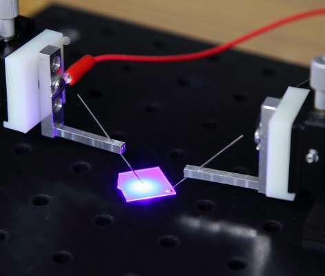
Gallium nitride (GaN)
GaN is a chemical compound of gallium (Ga) and nitrogen (N). GaN was developed as the material of blue LEDs. It has a high breakdown field strength and saturation speed of electrons. Research on GaN has recently been active because GaN is expected to be used in next-generation low-loss, high-efficiency, energy-saving power devices.
Power devices
Power devices are semiconductor devices used to convert voltage and frequency to control motors during the generation, transmission, and consumption of power (electric energy). They are used in various applications such as for power generation and transmission in substations, hybrid/electric vehicles, trains, and domestic appliances.
Silicon (Si)
Si is a single-crystal material that plays an indispensable role in many electric appliances supporting our lives, such as personal computers, televisions, and smartphones, and in social infrastructure, such as traffic and communication systems. It is widely known as a semiconductor.
Silicon carbide (SiC)
Research on the peripheral technology of SiC, in addition to that of GaN, which are used as semiconducting materials in next-generation power devices, is under way. Compared with conventional Si devices, SiC devices with a higher voltage tolerance and low loss can be fabricated, making them advantageous for high-voltage-tolerance and large-current applications such as those driven by motors.
Text extracted from “IMaSS NEWS Vol. 01” Special Issue, IMaSS Publicity Committee (Sakamoto and Konishi)