Can it be a semiconductor device?—I whispered out loud because Y. Ohno Lab’s devices are so thin and flexible. How could they work as semiconductors? What is “human affinity” proposed by Ohno Lab? How and where are carbon nanotubes (CNTs) utilized?
To seek answers to these questions, I got to have a talk with members of Y. Ohno Lab.
| What is a carbon nanotube? | |
| —– To start off, could you explain to me what a carbon nanotube is?
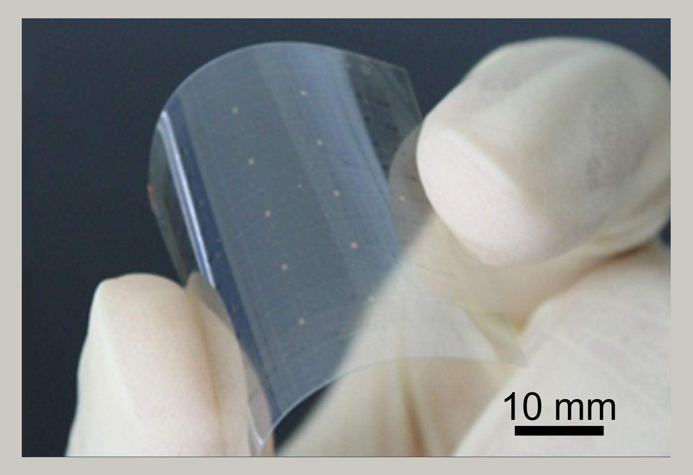
Ohno: Carbon atoms can be tightly bonded together in a hexagonal honeycomb lattice to form a thin material called graphene, which is only one atom thick. CNT is a graphene sheet rolled in an extremely thin cylindrical shape with a diameter of 0.4 to 50 nanometers*1. Carbon is lightweight, has strong tensile strength, and conducts heat better than anything else. Electrons traverse it very fast. It is a superb material. —– Where can CNTs be used most advantageously? Ohno We are currently working on flexible devices. They are transparent and stretchable, so they can be plastered on human body. This level of flexibility cannot be attained in conventional semiconductors. Humans, electronics, and semiconductors will be merged ever more deeply. In other words, cyberspace will converge with our living space, so we are expecting solid demand for flexible devices. That is our target. —– In some countries, you can embed a device in a human body. Ohno: Japan is not so lenient with human bodies. We need a lot of permissions. Yet skin surfaces are outside the regulations such as Pharmaceutical Affairs Law. Even from the surface, we can tell how much sweat has been secreted, so how much water and salt intake is necessary, or that someone is a bit tired. We can collect a lot of information and we can detect illness. Our first step will be an epidermal device that adheres to human skin to collect such information. |
 Professor Yutaka Ohno [profile] |
| Focus on human affinity | |
|
—– That is an advanced form of a wearable device. Is it like an adhesive bandage? Ohno: Deeper integration with cyberspace will require a lot of sensors attached to human bodies. We can wear them more comfortably if they are more transparent, thinner, lighter, and more flexible. We are expecting demand from healthcare, and surely from sports as well. When someone intends to move a muscle, myogenic potentials are evoked. When an athlete moves muscles, most important parts are activated whereas least important ones are relaxed. People who are helpless with sports, as well as people who are not good at musical instruments—they apply their energy in the wrong places. All these things can be visualized now. —– That seems to be why you describe these flexible devices as having human affinity. Ohno: Exactly. But I really want to create something like automatic medicine injection, something clinically applicable. For example, diabetes patients might stagger while walking when their blood glucose level falls, so they need glucose intake or injection. People with such risks live with concerns and mobility limitations, which we would like to address with automated solutions. There might still be a long way to go. —– For a solution to be adopted widely, cost can be an important issue. Ohno: CNTs are made of carbon, so there is existing technology to mass produce them at a lower cost. To use them in practical devices, however, we need a lot more basic research on materials and devices. Actually, we have already made significant progress, like integrated circuits for sensors which can now be fabricated entirely by CNT technology, and they are fairly stable. |
|
| Self-powered devices? | |
| —– As a next step, you thought of system construction and energy harvesting*2 as well.
Matsunaga: Yes. Energy harvesting means accumulating small amounts of energy to generate power, which is what I am currently working on. If we have a device affixed to human skin, a big question is how to power it. We don’t want a dangling wire, so why not collect available energy on the spot to power the system? —– How did you first conceive your idea of obtaining power from where nothing seems to exist. Matsunaga: I knew fluid power generation. Power is generated when water comes in contact with a CNT surface. That is where I started, like other people. When I actually experimented on it, I observed large power which was not explainable by the idea of water flow power generation. I gave it a thought and found that frictional electrification was the cause. This led me to harvesting energy from frictional electrification, or vibration power generation, which I am working on now. This is how I got to pursue this field. —– What is the current situation like? Matsunaga: Energy harvesting cannot provide enough power yet to wearable devices, for example. Much more power is necessary. If we attach it to a human arm, we need to bend and stretch our arm so strenuously. It is easiest if we attach it to the bottom of a foot. We need to think about what is best in terms of human movement, or where best to attach it. Among other things, we want to increase the power output of our devices. We cannot think about powering wearables without increasing the power. |
 Assistant Professor Masahiro Matsunaga [profile] |
|
Very simple structure |
|
| —– How is a power-generating sheet structured?
Matsunaga: Transparent rubber called PDMS, or dimethylpolysiloxane, contains a single CNT electrode. Nothing more. So simple. In its simplest form, the rubber incorporates a single CNT layer, about 40 nm thick, which contains networked CNTs at a density of 85%–90% approximately. Just by touching it, power is generated. —– It is awesome if we can use this energy to drive a device or dispatch data. Matsunaga: CNTs are normally produced as a mixture of semiconductors and metal in the ratio of 7 to 3. In order to use them for devices, there are issues like separating only semiconductor parts, but we can ignore these problems for electrodes. We can rather take advantage of CNT’s transparency, stretchability, durability, easy manufacturability, and the like. |
|
| All-carbon devices | |
| —– I have heard that you used to be a student member of Y. Ohno Lab. What did you do back then?
Uchiyama: When I was a student, I studied CNTs and diamonds to create devices for quantum information processing. That was my doctoral study. When I completed it, I moved to the University of Tokyo to work on new materials as a postdoctoral researcher. I studied molybdenum disulfide, a relatively new 2D material, i.e., an atomic layer material, to create devices. —– What are you focusing on now? Uchiyama: Back to CNTs. I would like to make use of 2D materials for flexible integrated devices, i.e., transistors, to implement circuits and systems. Something that can sense human heart pulses and take electrocardiograms. If it can detect any abnormality in electrocardiographic patterns and give advice like you want to go see your physician soon, that will be great. —– When you make all-carbon devices, where do you pay special attention? Uchiyama: CNTs are fairly much chemically resistant, so they are much easier to process compared to other organic materials. But there is hysteresis*3, like water on the surface of CNTs. Effects like this can affect electric properties of CNTs, so the key is to keep the surfaces of CNTs as clean as possible. Perhaps that is the most important. These days, with a parylene*4 or other tight cover and sufficient excitement, we can reduce hysteresis. |
 Assistant Professor Haruki Uchiyama [profile] |
| As easy as printing! | |
| —– What is so good about making all-carbon devices?
Ohno: We can make flexible devices without any precious metal. Actually, CNTs can be used in a mass printing process. We can already simply print integrated circuits. So it is low cost and customizable to our liking whenever we want it, … a lot of benefits. We are expecting that these benefits will be realized in five years’ time. —– I have heard that you have researched far and wide. Ohno: From physical property to material creation, devices, and integrated circuits, yes, I have gone far and wide. This experience seems to be bearing fruit now. If we endeavor to use this new material, CNT, to create devices for practical uses, we need to know much more than devices themselves. We need to know circuits and systems. This material is so new that a lot of aspects are yet to be discovered. —– So you are exploring more and more. Ohno: I think so. Getting intrigued, being focused, sinking in deep thought, and just pondering over whatnot, … I really treasure these moments. When I embark on a new thing and find something interesting or sense alternative possibilities, I get more deeply engaged and new ideas come up. And don’t forget casual talks with people who share these moments. Seemingly useless time is priceless in university research. |
|
[Glossary]
*1 nanometers:
1 nm (nanometer) = 0.001 μm (micrometer) = 0.000001 mm.
i.e., 1 nm equals a millionth of 1 mm.( ↑ back to main text)
*2 energy harvesting:
Energy harvesting refers to technology to collect, or harvest, small amounts of energy like light, vibration, and heat in order to generate and make use of electricity. ( ↑ back to main text)
*3 hysteresis:
A phenomenon where a system’s current state depends on the history of applied forces, not just the present ones.( ↑ back to main text)
*4 parylene:
Chemical compound. Parylene is a generic name for polymers with a para-benzenediyl ring as their main chain.(↑ back to main text)