AMTC
Organization
Advanced Measurement
Technology Center
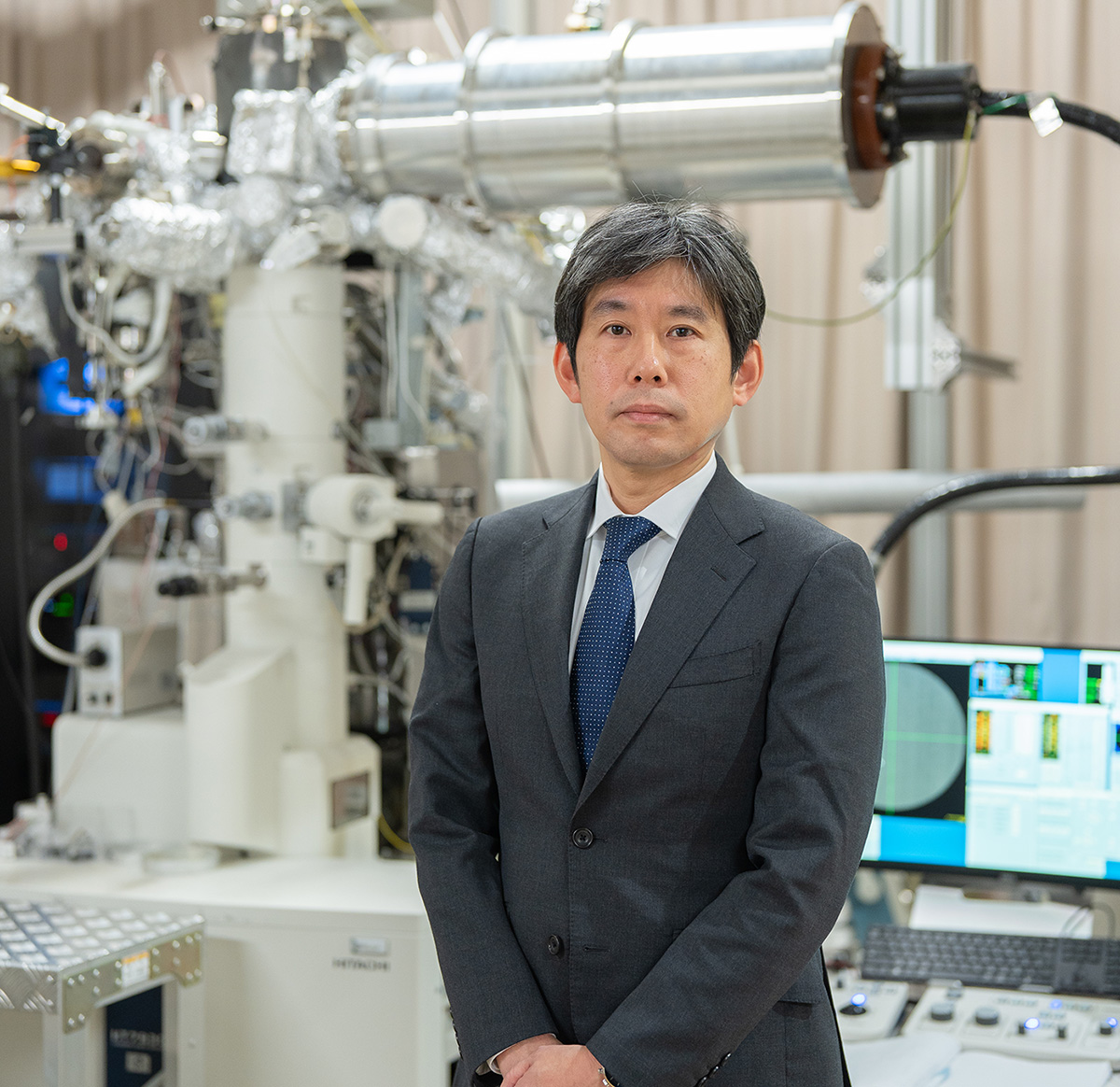
Advanced Measurement Technology Center
Director of AMTC
KUWAHARA, Makoto
This Institute has developed unique and advanced measurement technologies in the High Voltage Electron Microscope Laboratory, the Research Facility for Advanced Science and Technology, and other facilities of the Institute. The Advanced Measurement Technology Center, which was established in April 2015, aims to explore and develop novel measurement techniques, operate multiuser instruments, provide opportunities for collaborative research, and train highly skilled scientists and engineers. The Center is operated jointly by Nagoya University graduate schools and research centers with ties to this Institute, including the Graduate Schools of Engineering, Science, and Environmental Studies, and the Synchrotron Radiation Research Center, and external institutes, such as the Aichi Synchrotron Radiation Center of the Knowledge Hub Aichi, the National Institute for Fusion Science and Japan Fine Ceramics Center (JFCC). The Center is divided into the following five sections: Electron Nanoscopy Section, Electromagnetic Wave Measurements Section, Elementary Particle Measurements Section, X-Ray Spectroscopy Section, Nanofabrication & Characterization Section.
Advanced Measurement Technology Center
![]() Movie
Movie
Advanced Measurement Technology Center Introduction video
-
Creating new future materials and devices by measuring what is in front of you(2min.46sec.)
 Section / Group
Electron Nanoscopy Section
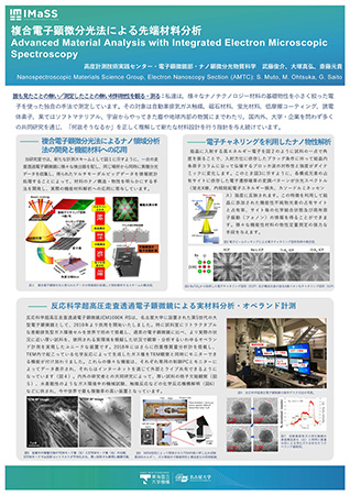
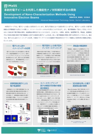
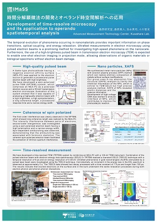
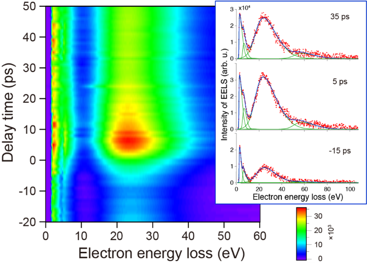
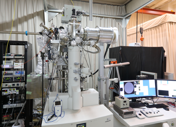
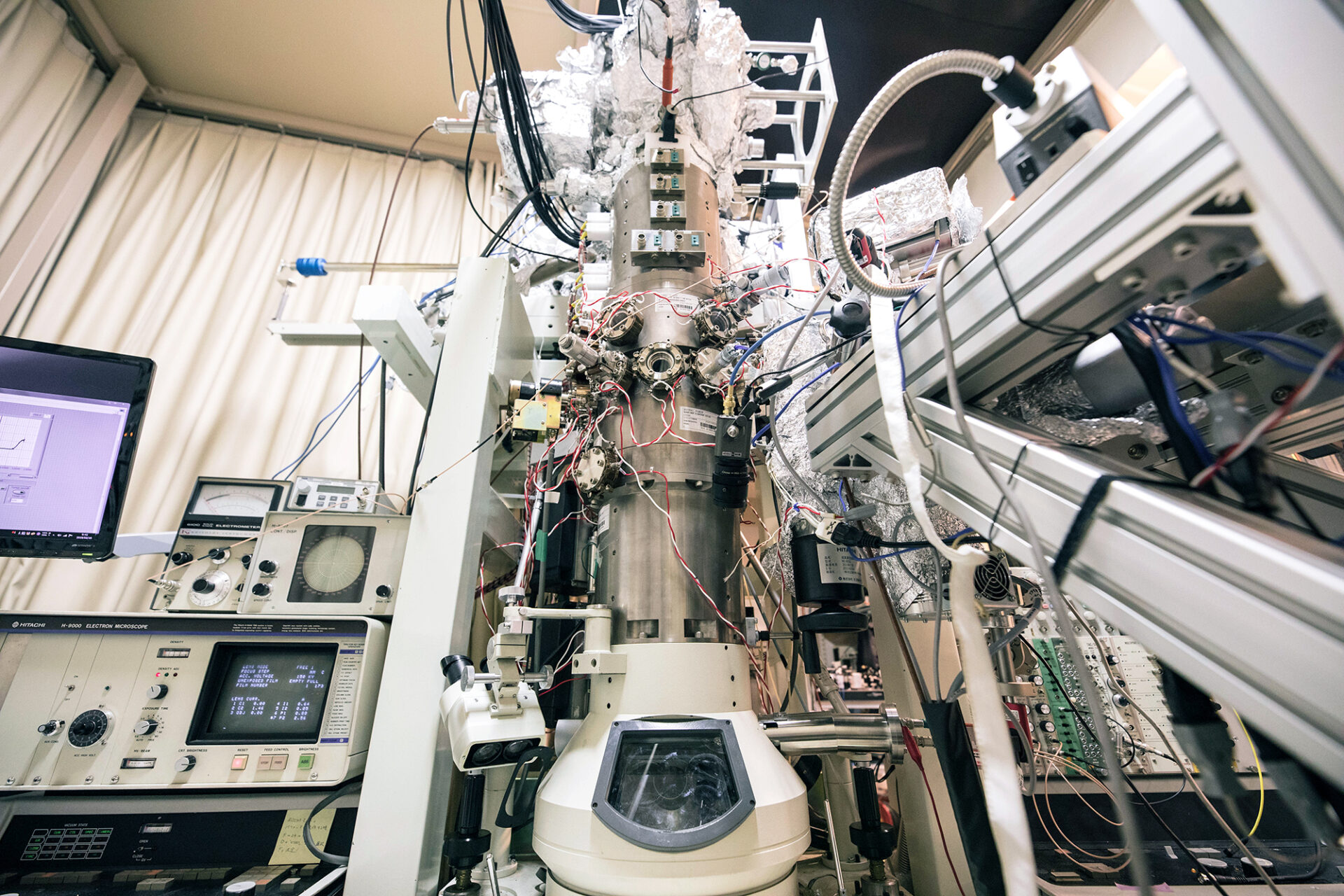
In this section, techniques for detailed structural analyses and property measurements using electron microscopes are developed; precise measurement of lattice strain in the nanometer range using convergent beam electron diffraction (CBED); three-dimensional structural analysis through electron tomography; visualization of electromagnetic fields and local strains using 4D-STEM technology with newly introduced detectors; operando observation and analysis of chemical reactions under gas environments; and time-resolved observation and analysis using pulsed electron beams.
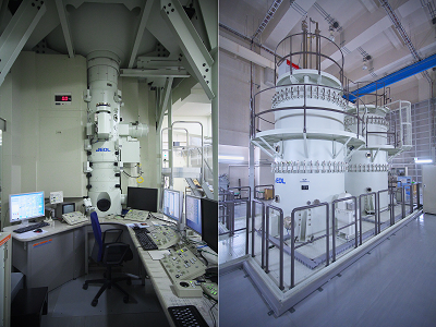
Reaction Science Ultra-High Voltage Scanning Transmission Electron Microscope JEM1000K RS
Nanospectroscopic Materials Science
In current practical materials related to nanotechnologies, defect formation associated with impurity doping and surface/interface structure control drastically improve their physical properties. Our research group is developing precise nano-area analysis methods using advanced electron spectroscopy/microscopy in combination with ‘informatics’ techniques to clarify the mechanisms behind the material functions and the guiding principles in the development of novel materials. Our research covers topics from fundamental physics such as measuring magnetic moments in sub-nanometer areas to the practical analysis of materials such as lithium ion batteries, catalysts for purifying automotive exhaust gas, ceramic devices, and ferrite magnets.
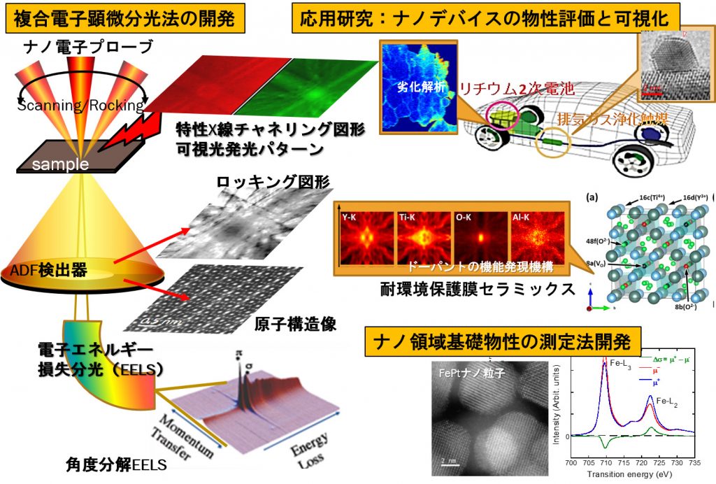
R&D of Sub-nanometric Scale Analysis by Integrated Spectroscopic Microscopy
Nanospectroscopic Materials Science / S. Muto & M. Ohtsuka
Electromagnetic Wave Measurements Section
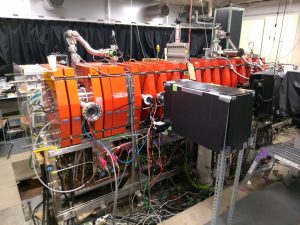
This section is dedicated to the advancement of techniques to control energy systems, such as nuclear fusion using plasmas. Research is focused on developing methods to measure electromagnetic waves and reflected light from emitting bodies and materials, including plasma diagnostics observing line emissions from atoms and molecules and using lasers.
Plasma Energy Engineering
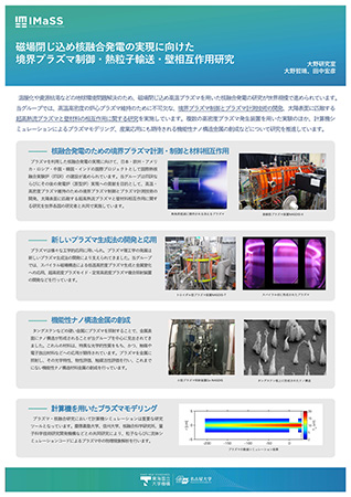
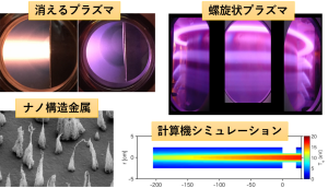
To address global environmental challenges such as global warming and resource depletion, research on fusion power generation using magnetically confined high-temperature plasmas is being conducted on a global scale. Our group is engaged in the development of edge plasma control techniques and advanced plasma diagnostics, both of which are essential for the stable maintenance of high-temperature, high-density core plasmas. We are also conducting research on the interaction between wall materials and ultra-high heat flux plasmas, with intensities comparable to those on the solar surface. These studies are carried out through experiments using high-density plasma devices, as well as through computational plasma modeling using numerical simulations. In addition, we are working on the fabrication of functional nanostructured metals with promising potential for industrial applications, thereby promoting a wide range of research from fundamental science to practical technologies.
Member
-
Project
Edge Plasma Control for Magnetically Confined Fusion Power Plant
-
Project
Research on Heat and Particle Transport in Edge and Divertor Plasmas for Thermonuclear Fusion Power Generation
-

Elementary Particle Measurements Section
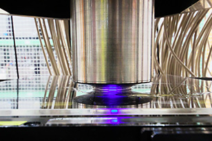
Hyper Track Selector
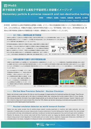
This section specializes in the development of muon radiography, which is an applied technology to obtain images inside extremely large structures (e.g., pyramid, nuclear reactor, blast furnace, volcano). This technology makes use of muons, which are elementary particles found in charged cosmic rays from outer space that hit the Earth, and other in-house conceived techniques.
Instrument Development
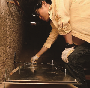
- Nagoya University emulsion film setup in the descending corridor
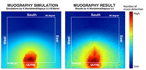
- Comparison of muography simulation and results for descending corridor
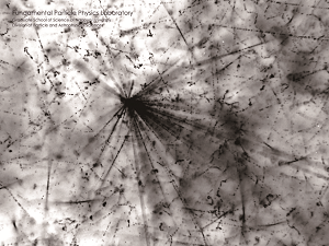
- This micrograph showing the reaction that occurred when high-energy cosmic rays collided with atoms in the emulsion.
Member
-
Project
Research on the development and promotion of advanced nuclear emulsion technology and the development of applications using this technology
-
Project
Development of Innovative High- Resolution Three-Dimensional Radiation Detector “Nuclear Emulsion” Technology and Its Applications
-
Project
Neutrino Oscillation, Dark Matter Search Experiment and Researches with Tracking by Nuclear Emulsion
-
Project
R&D of cosmic ray imaging techniques with nuclear emulsion
-
Project
Study of Gravity and Unknown Short-range Forces Using Nuclear Emulsion and Quantized States of Ultracold Neutrons, Development of Nuclear Emulsion Gels, Development of Nuclear Emulsion for Slow Neutrons, and Development of Nuclear Emulsion for X-ray Topography
-

Designated Assistant Professor
MATSUO, Tomokazu
-

Researcher
ISHIGURO, Katsumi
-

Researcher
YAMAMOTO, Saya
-

Researcher
HAYAKAWA, Tomohiro
X-Ray Spectroscopy Section
In this section, research studies using sophisticated of X-ray spectroscopy techniques and their complex technologies combined with coherent electron beams are conducted toward developing functional materials and pharmaceuticals.
Nano Dynamics
Leveraging dynamic measurement technology using X-ray and electron beam, we clarify properties of devices and materials in actual operating condition to accelerate development of energy-saving technologies. Furthermore, we will explore the frontier of measurement technology that combines electrons and photons.
Member
-
Project
Advanced Electron Microscopy Using Coherent Spin-Polarized Pulse Beam
-
Project
Nanostructure modelling of energy material by multiprobe composite analysis
-

Visiting Professor
AGEMURA, Toshihide
-

Visiting Professor
TOGAWA, Kazuaki
-

Visiting Associate Professor
NOMAGUCHI, Tsunenori
-

Visiting Associate Professor
MORISHITA, Hideo
-

Project
Catalytic reaction mechanism analysis using in situ electron microscopy, mass spectrometry, and machine learning
Nanofabrication & Characterization Section
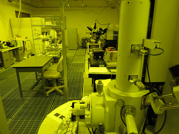
Micro-fabrication clean room
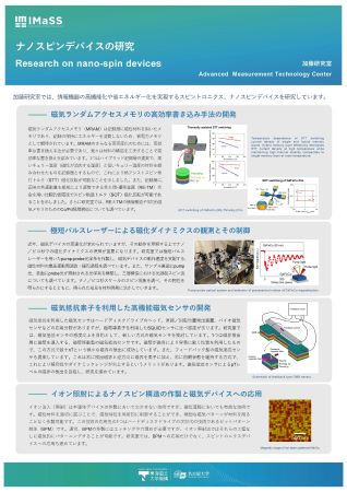
This section develops the state-of-arts techniques of thin-film deposition, nanomaterial synthesis, nanofabrication, and associated measurements and evaluations. Shared instruments and clean room at Research Facility for Advanced Science and Technology are provided for the development of advanced functional devices.
Nano-Spin Devices
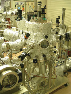
Magnetron sputtering with 8 sources
Member
-
Project
Developments of Functional Magnetic Thin Films and Spintronics Devices
-
Project
Development of Fabrication Process of Micro Magnetic Pattern and Its Application
-
Project
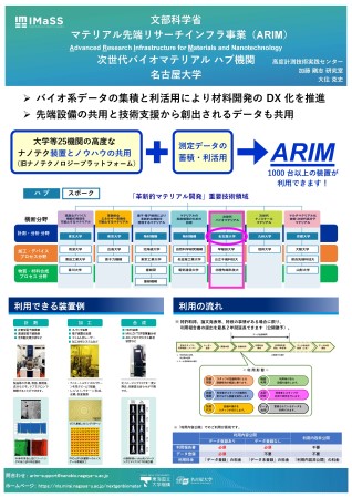
Research and technical support of Advanced Research Infrastructure for Materials and Nanotechnology, Development of semiconductor measurement technology and application
-

Project
Research and technical support of Advanced Research Infrastructure for Materials and Nanotechnology
-

Visiting Professor
SONOBE, Yoshiaki
ナノ構造制御学
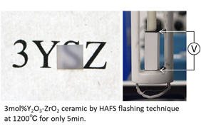
様々なセラミック材料の特性の多くは、表面・結晶粒界・界面などの格子不整合領域における原子構造・電子状態と密接に関係しています。本研究グループは、このような機能をつかさどる格子不整合領域に着目し、透過型電子顕微鏡を用いたナノ領域の直接観察・分析技術をもとに、主にセラミックを対象とした新規材料開発や 新たな焼結プロセスの開発を行っています。
Member
-
Project
Development of Ceramic Materials by Controlling the Atomic/Electronic Structures at Nano Scale


