Research
Research Group
Interview with Ujihara Lab
Diversity is a Hallmark of Our Laboratory
— Can We Bring about a Revolution in the Global Energy Scene? —
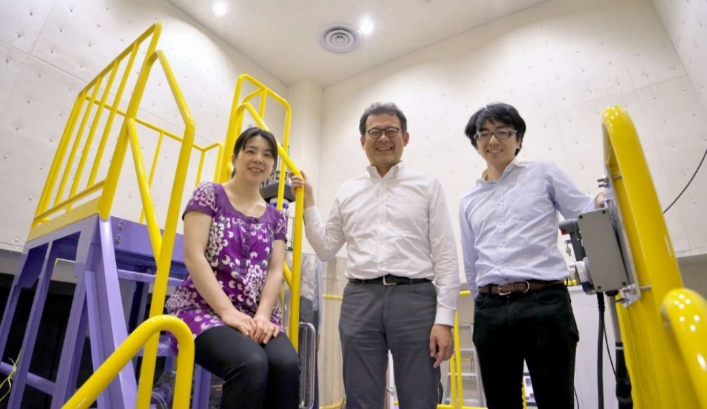
(From left to right) Associate Professor Tagawa, Professor Ujihara, and Dr. Harada (lecturer)
In line with its portrayal as a diverse lab, Ujihara Lab consists of multifaceted and multitalented members who are pursuing research on a variety of materials that will bring about a revolution in the global energy scene. Their key goal is crystal growth, i.e., the production of fine crystals.
In this interview, we listen to three researchers about their work, including why the production of fine crystals is necessary.
Key goal of crystal growth
A compound called silicon carbide (SiC) is the main research material in the Ujihara Lab, isn’t it?
Actually, we also study materials other than SiC. But you’re right, SiC is our first priority. SiC is critically important as a semiconductor material that can solve energy problems. The three major challenges currently facing the world are water, food, and energy. Most of the members of our laboratory are involved in research on the growth of energy-related crystals, in other words, the production of fine crystals.
How much energy will be saved when a fine SiC semiconductor with good performance is achieved?
Semiconductors are used everywhere from trains to elevators, electric vehicles, and motors in large plants. According to an estimate by the government, the amount of energy saved in Japan alone will be equivalent to the energy generated by 10 nuclear power plants. The problem is that semiconductors are still expensive. To decrease prices, it is essential to improve the quality of crystals.
Achieving a big breakthrough using AI in simulations
It’s easy to say but hard to do.
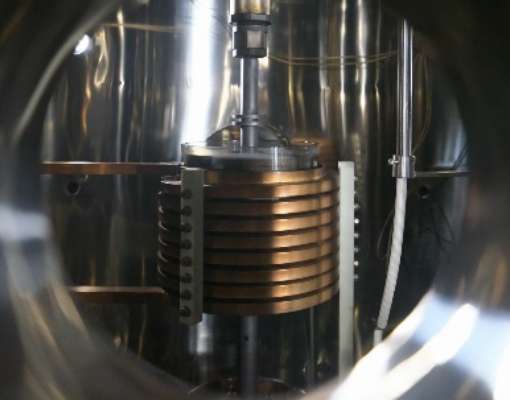
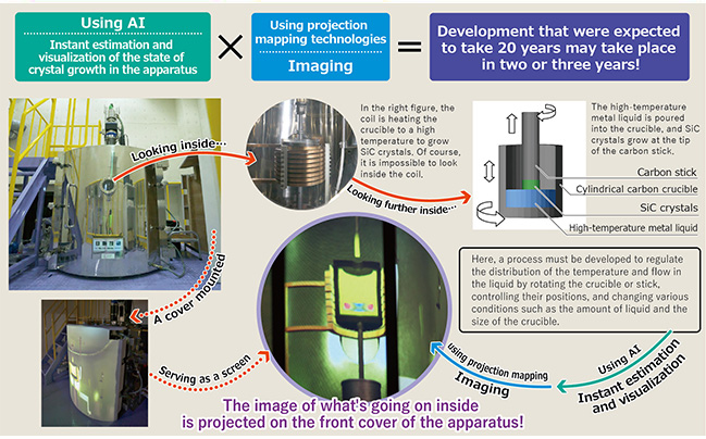
I’m sure that the SiC crystals we are making are the finest in the world, but the biggest problem is that we can still only make small crystals of 10 or 15 mm in size. However, as a result of using AI in simulations of production, the rate of development has significantly increased. Developments that were expected to take 20 years now look as if they will take place in two or three years. Moreover, the state inside the apparatus when the temperature is higher than 1,000 °C has been visualized by animation projections. Even in situ measurements have become possible.
Utilizing self-assembly in crystal growth
How do you describe the crystallization of DNA molecules?
This involves taking advantage of the nature of DNA by bonding DNA molecules, which are also found in our body, to nanoparticles so that the nanoparticles crystallize as planned. Because DNA has a base sequence, we can design and control the arrangement, in other words, whether or not a molecule binds to a certain molecule. Heat retention is required during crystallization, so we use a vacuum thermal insulation pot such as the one used for making curry. All we have to do is stir it lightly. Such self-assembly is very economical and environmentally friendly.
Would you give us an example of what you can do with this technique?
For example, the wavelength of light is limited to a certain range, so there is a limit to the type of light we can deal with. However, the light confined in the nanoregion of the nanoparticle ensembles we are making has very different properties from those of ordinary light. Taking advantage of such properties, in principle, we may see atoms and molecules that could not have been seen with an optical microscope.
Diversity is the laboratory’s hallmark
By the way, there are a variety of talented people including female researchers in Ujihara Lab.
We are diverse! Our laboratory consists of people of almost all ages, including children younger than 10 (just joking) and those in their 70s, although there are no people in their teens or 60s. There are also lab members from China, Taiwan, and Korea, and we used to have people from India. Actually, we’d like to accept people from all over the world. Young people see Dr. Tagawa’s children playing in our laboratory room and think that is normal. Then they go back out into the world, where there may be no such supportive environment for researchers with children at their workplaces, but they can make a change by asking, “Why not?”
Semiconductors
The term “semiconductor” focuses on a specific electric conduction property of a material. Smaller and lighter semiconductors with higher performance are desired. Generally, the term “semiconductor” refers to a “semiconductor integrated circuit”. Semiconductors are used in all types of product from digital appliances, such as PCs, smartphones, and liquid crystal TVs, to household appliances, such as refrigerators and washing machines, and vehicles. Also, semiconductors are widely used in railway traffic control systems, banks and brokerage houses, and the control of social infrastructure including electric power, gas, and water. It is now difficult to live without semiconductors. In addition, with the recent spread of IoT, the amount of digital data has increased markedly. As a result, a tremendous number of servers, which use a large number of semiconductors, are required to store such big data. The global semiconductor market is growing rapidly.
Written by Publicity Committee of IMaSS (Okada and Konishi) — Excerpt from feature article in “IMaSS NEWS Vol.05” —